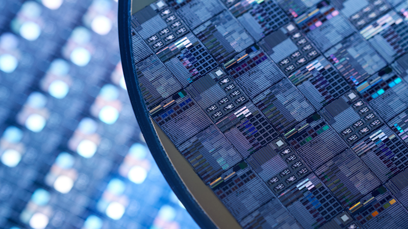
Application of Atomic Force Microscopy in the Study of Semiconductor Materials and Devices
Thank you. Your on-demand video is now available.
DNA-PAINT is a localization-based super-resolution method offering molecular resolution (< 5 nm) combined with unlimited multiplexing capabilities. DNA-PAINT reagents from Massive Photonics are a perfect match for the Bruker Vutara VXL microscope. In combination with the Bruker fluidic system, automated, multiplexed cellular imaging in 3D is now accessible out of the box.
Watch the webinar for practical guidance for DNA-PAINT sample preparation, image acquisition, and data analysis, as well as an introduction to:
- The Vutara VXL super-resolution microscope and integrated fluidics unit;
- The theoretical background of DNA-PAINT; and
- The products available from Massive Photonics for DNA-PAINT experiments.
If you have any questions about these or any of our other products or services, please contact us. Follow @BrukerFM on Twitter for event, product, and webinar updates.
Key Topics
Our speakers take a closer look at the capability of industry-leading AFM technology to perform high-resolution imaging of surface topography. A few typical applications are covered, including:
- Roughness characterization of bare wafers and thin films;
- CMP characterization including roughness, dishing and erosion;
- Inspection of nanoscale defects; and
- Critical dimension metrology of lines, trenches, holes and other nanoscale structures such as CMOS imaging sensor micro lenses and LED patterned sapphire substrate dome structures.
Practical aspects such as tip selection, tip shape monitoring and tip lifetime, throughput, automation and extraction of critical analysis parameters are also discussed.
Finally, the webinar closes with an exploration of the capability to apply AFM for local chemical identification by combining it with nanoscale IR imaging and spectroscopy. Two interesting applications of this ‘AFM-IR’ approach are the chemical identification of contaminants and chemical mapping (with 10 nm spatial resolution) of specific materials.
This webinar was presented on: December 16, 2020
Speakers
Peter De Wolf, Ph.D.,
Director of Technology & Application Development

Ingo Schmitz, Ph.D.
Technical Marketing Engineer, Bruker