EN
My Bruker
Contact Expert
Products & Solutions
Applications
Services & Support
News & Events
About
Careers
Please use at least 2 characters (you are currently using 1 character)
Languages
Deutsch
English
Español
Français
Italiano
Polski
Português
Русский
中文
日本語
한국어
Test & Measurement
High-performance surface and dimensional analysis tools for industry and researchers
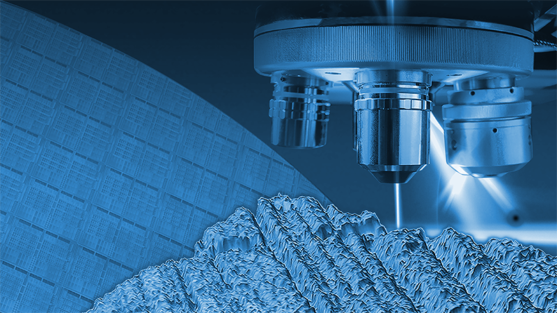
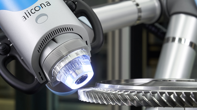
3D Optical Profilers
Non-contact 3D surface measurement, inspection, and analysis
Read More
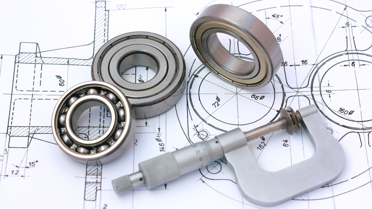
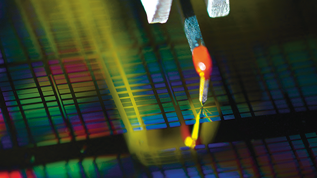
Dimensional Metrology Systems
Industrial quality assurance in all branches of precision manufacturing
Read More
Ellipsometers and Reflectometers
High-accuracy film measurement well beyond the thickness range and refractive index resolution of traditional ellipsometers/reflectometers
Read More
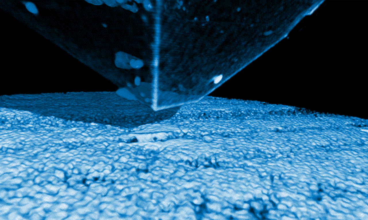
Nanomechanical Instruments for Microscopes
Equipment for nanomechanical and nanotribological testing in conjunction with Raman, XRD, Optical Microscope, and AFM techniques
Read More
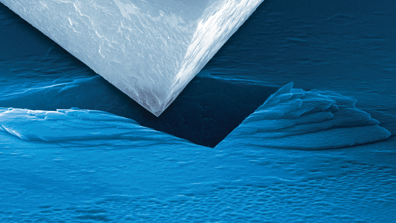
Nanomechanical Instruments for SEM/TEM
Hysitron PicoIndenters for in-situ mechanical experiments in scanning electron and transmission electron microscopes
Read More
Nanomechanical Test Systems
Stand-alone solutions for highly accurate and reliable quantitative mechanical and tribological characterization at the nano- and microscales
Read More
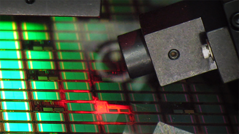
Stylus Profilometers
Surface roughness characterization, step height measurements, and film stress analyses
Read More
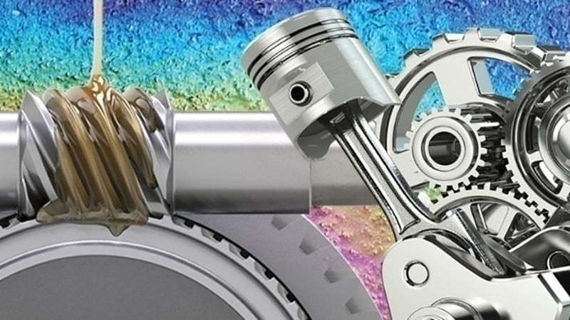
Tribometers and Mechanical Testers
Testing and measurement of friction, wear, and material mechanical properties
Read More
News
Read the Latest News