3D 광학 프로파일러

컨투어X-100

거칠기 계측을 위한 최신식의 경제적인 benchtop

ContourX-100

ContourX-100 광학 현미경은 Entry 설비로 동급 최고의 성능으로 정확하고 재현성이 월등한 비접촉 표면 측정법을 위한 새로운 기준을 제시합니다. 컴팩트한 설비 사이즈의 시스템은 수십 년 간의 브루커 백색 간섭계(WLI) 혁신을 통합한 최신 패키지로 2D/3D 고해상도 측정 기능을 제공합니다. 차세대 향상된 기능에는 새로운 5MP 카메라와 보다 큰 스테이지에 더불어 정밀한 가공 표면, 투명 막 코팅 및 트라이볼로지 응용에 대한 훨씬 더 큰 편리성과 유연성을 제공하는 새로운 측정 모드인 USI를 포함하고 있습니다.

업계 최고
Z 해상도
배율에 관계없이 일정하고 정밀한 측정 제공
타의 추종 불허
계측 값
성능 저하 없이 간소화된 설계 제공
사용자 친화적
소프트웨어 인터페이스
사전 프로그래밍된 필터 및 분석의 광범위한 라이브러리에 직관적인 접근 제공
See the ContourX family brochure and ContourX-100 datasheet for more information.
Download Now
기능

비교할 수 없는 계측

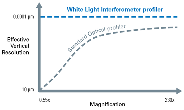
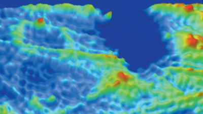
WLI는 모든 물체에 대해 일정한 최고의 수직 해상도를 제공합니다.

ContourX-100 프로파일러는 비접촉 표면 계측, 특성화 및 이미징 분야에서 40년 이상 쌓아온 독점적인 광학 혁신 및 업계 리더십의 정점입니다. 이 시스템은 단일 획득에서 다중 분석을 위해 3D WLI 및 2D 이미징 기술을 활용합니다. ContourX-100은 모든 표면 상황에서 0.05%부터 100% 반사도까지 견고합니다.

타의 추종을 불허하는 가치 및 분석

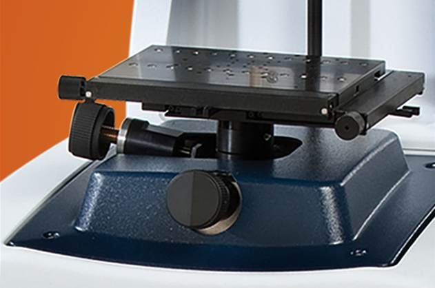
ContourX-100 수동 스테이지

수천 개의 맞춤형 분석과 브루커의 간편하고 강력한 VisionXpress™ 및 Vision64® 사용자 인터페이스를 갖춘 ContourX-100 benchtop은 실험실과 작업 현장 모두에서 생산성에 최적화되어 있습니다. 하드웨어와 소프트웨어가 결합되어 최고 수준의 고 처리량 광학 성능에 대한 간소화된 액세스를 제공하여 유사한 계측 기술을 완전히 능가합니다.

Applications

Surface-Independent Metrology with Application-Specific Solutions

Precision Engineering

Keep the surface texture and geometric dimensions of precision-engineered parts within tight specification limits. Our gage-capable measurement systems provide efficient feedback and reporting as you monitor, track, and evaluate processes and assess GD&T conformance.

MEMS and Sensors

Perform high-throughput, highly repeatable etch depth, film thickness, step-height, and surface roughness measurements, as well as advanced critical dimension metrology of MEMS and optical MEMS. Optical profiling can characterize devices throughout the manufacturing process from wafer to final test, and even through transparent packaging.

Orthopedics/Ophthalmics

Obtain precise, repeatable measurements of implant materials and components through the complete product life cycle. Our WLI optical profilers support R&D, QA, and QC analyses, for applications ranging from characterization of surface parameters of lens and injection molds to surface finish verification and wear of medical devices.

Tribology

Measure, analyze, and control the impact of friction, wear, lubrication, and corrosion on material/component performance and lifespans. Determine quantitative wear parameters and perform fast pass/fail inspections on the widest range of shiny, smooth, or rough surfaces.

Semiconductors

Improve yield and reduce costs for both front- and back-end manufacturing processes with automated, non-contact, wafer-scale metrology systems. Perform post-CMP die flatness inspection; bump height, coplanarity, and defect identification and analysis; and measure the critical dimensions of component structures.

Optics

Better understand the root causes of defects and optimize polishing and finishing processes with accurate and repeatable sub-nm roughness measurements. Our non-contact metrology systems enable compliance with increasingly stringent specifications and ISO norms for samples ranging from small aspheric and free-form optics, to optical components with complex geometries, to diffraction gratings and microlenses.

문의

Input value is invalid.

* Please fill out the mandatory fields.

Please enter your first name
Please enter your last name
Please enter your e-mail address
Please enter a valid phone number
Please enter your Company/Institution
What best describes your current interest?
Join our email subscription list to receive related webinar invitations, product announcements, and information about upcoming events near you.
Please accept the Terms and Conditions