In-situ Element Mapping at Elevated Temperatures
Electron microscopy is the means to study materials with high spatial resolution. Energy dispersive X-ray spectroscopy (EDS) in the electron microscope allows to map element distributions on the nanoscale. And finally, the use of heating holders, or any other in-situ reaction cells, which are suitable for electron microscopy and EDS, allows to monitor the effect of materials treatment in-situ or in-operando in the electron microscope. This means that information on changes in structure and element composition is available qualitatively and quantitavely with high spatial resolution.
A Pt-Pd test specimen was investigated at various elevated temperatures using the Wildfire, a MEMS based heating holder from DENS solutions and a Bruker QUANTAX EDS system with an XFlash® 6T 30 detector on a standard scanning transmission electron microscope (STEM). The detector with 30 mm2 active area achieves a collection angle of 0.09 sr at a take-off angle of 22° in the STEM used. The specimen holder is of a new special design for improved thermal stability in z-direction, which allowed to monitor the same specimen area easily between room temperature and 1000°C. The EDS system provided suitable mapping times of a few min element map at each temperature step.
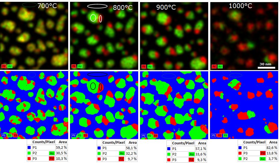
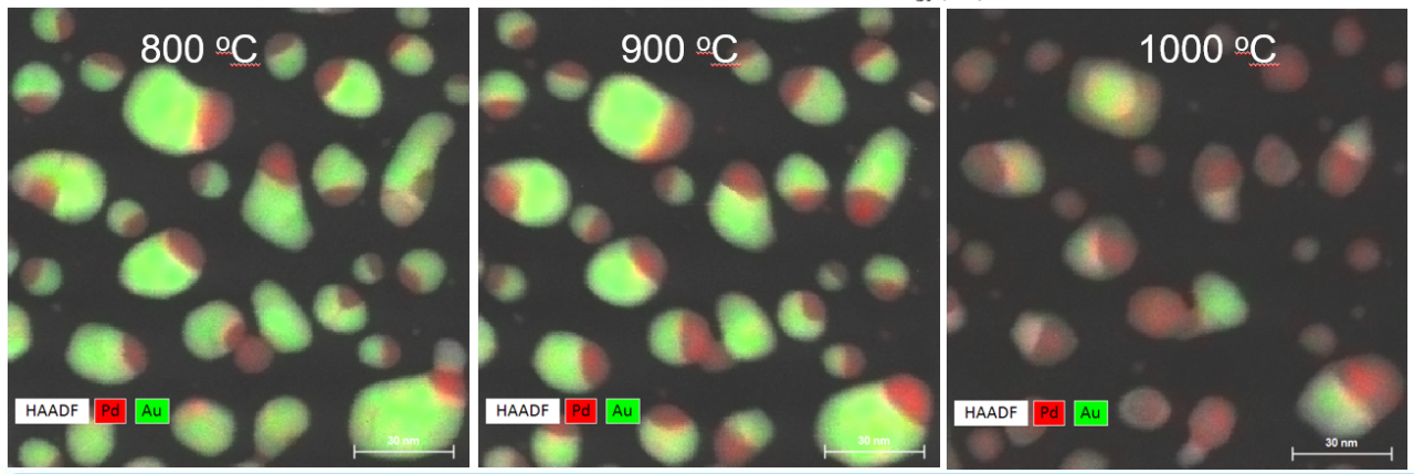
Figure 1 shows the development of the Pt-Pd nanoparticles with rising temperature.
Figure 2 demonstrates how the development of the particle number size and composition can be monitored quantitatively using PCA based phase analysis and arealy coverage.