In situ TEM observation of rebonding on fractured silicon carbide
Nanoscale, 2018
Silicon carbide is a unique semiconductor utilized in a variety of demanding applications where it can be exposed to extreme environments, such as high-power operation and elevated temperatures. The mechanical reliability of such devices must also be well understood to optimize device lifetime, where failure generally occurs by brittle crack growth. One means in which failure by crack growth can be partially mitigated is through crack healing. Crack healing is an interesting process where bonds can be repaired across a closed crack, and is generally assisted by electrical, thermal, and chemical means.
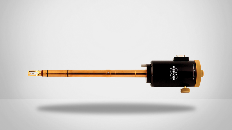
This study reports on in situ TEM tensile testing of both amorphous and single crystal SiC nanowires using a Hysitron PI95 TEM Picoindenter and the push-to-pull (PTP) device. The nanowires were prepared using a novel approach with an eyebrow hair as the manipulator, together with silver-filled adhesive to avoid potential FIB damage. Both types of nanowires exhibited multiple crack healing and re-fracture events. This was examined in greater detail using high-resolution TEM and molecular dynamics simulations. The mechanism of crack healing was found to be atomic diffusion, which underwent partial recrystallization and recovered a portion of the original nanowire strength. Since this was done in a vacuum, the fracture surfaces did not oxidize and the reduction in surface energy drove the healing process requiring, no external energy input.

