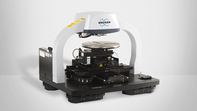
Surface Characterization of Semiconductor Materials and Devices
Learn everything about stylus profilometry for semiconductor applications, from fundamentals to a real-time demonstration
Leveraging stylus profilometry for semiconductor research and manufacturing
PRESENTATION HIGHLIGHTS:
- [00:00:00] Introduction to stylus profilometry
- [00:01:27] Stylus profilometry main capabilities
- [00:03:31] Solution for step height & thin films
- [00:04:50] Solution for bow & thin film stress
- [00:05:57] Semiconductor and microelectronics applications
- [00:06:49] Vision64 software demonstration
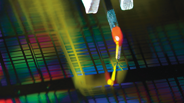
Stylus profiling for high vertical resolution and long-range flatness measurements
PRESENTATION HIGHLIGHTS:
- [00:00:00] Step Height and Thin Film
- [00:02:17] Bow and Thin Film Stress
- [00:04:13] DektakXT demonstration