Application Note: High-Throughput Full-Die Nanoscale Topography Using AFM
Extending Local AFM Precision to Wafer-Scale Process Control
As semiconductor devices scale in complexity and size, metrology at the nanometer scale has become critical. Traditional atomic force microscopy (AFM) excels at producing high‑resolution results but typically only covers up to about a 100x100 μm area. Bruker’s Large‑Area Scanning and exclusive, patented HyperMap™ technologies provide the ability to far surpass this field‑of‑view constraint, bridging the gap between localized AFM precision and wafer‑scale process control.
This application note explains the working principles of Large‑Area Scanning and HyperMap, then presents case studies showing full‑die topography data collected using Large‑Area Scanning, and hotspot inspection with HyperMap.
Readers can expect to learn how to:
- Use Large‑Area Scanning to capture long‑wavelength topography variation across full‑die dimensions
- Apply HyperMap to identify and inspect post‑CMP hotspots in targeted regions of interest
- Connect full‑die nanoscale topography metrology to faster feedback for wafer‑scale process control
KEYWORDS: Atomic Force Microscopy; Large-Area Scanning; HyperMap; Semiconductor Metrology; CMP; Hybrid Bonding; Full-Die Topography; Inline Inspection; AFM Metrology; InSight AFP-HB; Application Note

Why Large‑Area Metrology Is Critical for CMP and Bonding Performance
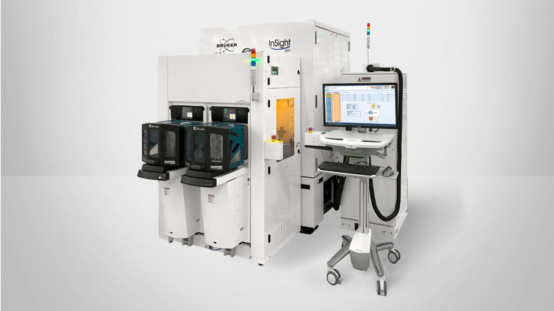
Large‑Area Scanning and HyperMap on InSight® AFP‑HB (Figure 1) equip semiconductor manufacturers to retain high vertical and planar resolution while capturing long‑wavelength variations across larger areas, such as a full die. Topography variations at these larger, millimeter scales can significantly impact chemical mechanical planarization (CMP) processes, and thus also hybrid bonding, lithography, and packaging. Recent studies highlight that within‑die non‑uniformity (WiDNU), pattern density dependencies, and long‑range planarity issues are increasingly difficult to manage, especially as die sizes approach 800 mm² and beyond.1,2 These topographical inconsistencies manifest as dishing, erosion, and surface topography variations that are detrimental to bonding integrity and device yield. Hybrid bonding is particularly sensitive to such topographical defects and therefore requires ultraflat surfaces across both copper and dielectric regions at the local scale, as well as planarity over millimeter scale lateral distances within a die. Combining nanometer scale vertical resolution with millimeter scale lateral coverage provides the metrology capability needed to characterize and manage these multi‑scale topography challenges.
Historically, post‑CMP hotspot inspection was performed using white light interferometry (WLI). While effective in certain contexts, this technique is limited by material dependencies and typically requires a reflective coating to avoid artifacts caused by the presence of dissimilar materials. As a result, wafers must be removed from the production flow, coated, and then inspected — introducing significant delays and sacrificing valuable product wafers for each measurement. This metrology loop not only impacts throughput but also introduces uncertainty and cost, driving the need for a faster, nondestructive alternative that can operate inline and at production speed.3
Large‑Area Scanning and HyperMap technologies enable inline, nondestructive nanoscale topography mapping across full‑die and multi‑die regions. These methods bridge the gap between localized AFM precision and wafer‑scale process control, offering manufacturers tools to detect, understand, and mitigate millimeter‑scale CMP‑induced variations.

Overcoming Conventional AFM Scan‑Range Limitations
Typical lateral (XY) AFM mode scan ranges for InSight AFP‑HB span from hundreds of nanometers to 105x105 μm. Larger fields of view can be covered using one of two approaches:
- Collect multiple images and stitch them together—a time‑intensive method that negatively impacts throughput.
- Raster‑scan the sample beneath a stationary probe using a fast, high‑precision stage. In this way, the accessible scan area expands to become as large as the available travel range of the stage — even covering a 300 mm wafer surface in full. The map in Figure 1 represents the field of view, spatial frequencies, and height ranges covered by InSight AFP‑HB using this method.
Bruker’s two advanced methods for performing large‑area AFM metrology are Large‑Area Scanning and HyperMap. Basic principles and example data for each are presented below.
Large Area Scanning for Unprecedented Lateral Coverage
Large‑Area Scanning can be conceptualized as a high‑precision, large‑scale implementation of AFM — essentially a scanning‑sample AFM configuration that enables unprecedented lateral coverage. During a large‑area scan, the sample is raster‑scanned beneath a stationary probe using a precision air bearing stage. At the same time, the Z‑piezo actuator maintains closed‑loop feedback to track surface height using standard AFM feedback mechanisms. The probe operates in oscillatory feedback mode, similar to conventional TappingMode AFM. As the sample moves under the probe, changes in surface height modulate the oscillation amplitude, which is used to maintain tip–sample interaction and reconstruct the topography with nanometer‑scale resolution.
Additional elements of Large‑Area Scanning that enable accurate, reliable metrology are:
- Continuous scanning — The scan is executed as a single, uninterrupted operation. Retracting the probe between scan lines disrupts measurement continuity and compromises spatial registration between lines.
- Reference‑plane acquisition — Prior to the high‑resolution scan, a low‑resolution reference scan is performed. This reference serves as a baseline for post‑acquisition leveling, ensuring that the final topography data are free from stage‑induced tilt or drift.
- Feedback dynamics optimized for scale and throughput — While similar to traditional TappingMode AFM, the closed‑loop feedback dynamics are optimized for throughput over the larger length scales of Large‑Area Scanning, together with application‑specific probe designs.
Together, these design principles allow InSight AFP‑HB to deliver high‑resolution, large‑scale topography maps that are critical for advanced semiconductor process control, especially in applications such as CMP characterization and lithography alignment. Importantly, the vertical resolution of large‑area scans remains equivalent to that of standard AFM, preserving nanometer‑scale sensitivity. Lateral resolution is user‑configurable and typically optimized based on throughput requirements and application‑specific needs.
LEARN MORE:
Figure 2 shows an example of Large‑Area Scanning on a commercially available metrology test wafer (AMAG7).4 The 7x7 mm scan contains 700 lines and 8412 pixels/line. Line sections at a few selected positions (Figure 2b) illustrate the capability to observe small variations in height over large areas. Figure 2c displays a digital zoom covering an area of 1x1 mm, showing good correlation with a separate (conventional) 100x50 μm AFM scan of the same area, as illustrated by the images and section profiles in Figure 2d and e.

Balancing Coverage, Resolution, and Throughput with Large‑Area Scanning
Large‑Area Scanning offers flexible options for adjusting scan area, resolution, and acquisition time, making it suitable for diverse semiconductor metrology tasks in both process development and high‑volume manufacturing (HVM), including CMP process monitoring and lithography focus control.
In process control scenarios, nanoscale topography over millimeter length scales can be the difference between yield and rework — or, worse, scrap. In many such cases, ultrahigh lateral resolution is not required, and a lower‑resolution scan can be completed within minutes, providing sufficient metrology for timely process decisions.
Alternatively, certain applications necessitate the detection of localized surface features, such as wiring‑density‑induced hotspots or clusters of defects. These scenarios demand higher lateral resolution, while acquisition time may be a secondary consideration. InSight AFP‑HB meets these requirements by supporting submicron line spacing, allowing for detailed characterization of small‑scale features.
Large‑Area Scanning Case Study: Hybrid Bonding
Figure 3 shows a second example, directly related to a real‑world wafer‑to‑wafer hybrid bonding issue. Post‑bonding inspection using confocal scanning acoustic microscopy (CSAM) revealed persistent multimillimeter scale voids between bonded wafers. These defects were only detectable after the wafers had been permanently joined, making corrective action impossible and resulting in costly wafer loss.
By scanning the entire 26x33 mm die, Large‑Area Scanning identified that regions with elevated topography correlated to variations in underlying layer density, which were the root cause of bonding voids. With this insight, the device manufacturer isolated a critical region of interest and reduced the scan area to a targeted 18x6 mm zone, enabling faster acquisition times that made it feasible to integrate Large‑Area Scanning into the regular production monitoring cycle.
Figure 3a and b show the same region, imaged using the same recipe, scanned before and after CMP process improvement. The change resulted in a measurable reduction in long‑range topography from 25 nm to 15 nm. The topography data provided by Large‑Area Scanning allowed the manufacturer to tune their CMP process, mitigating excess topography and significantly improving bonding quality and device yield. Today, Large‑Area Scanning has become a standard part of their post‑CMP metrology workflow, ensuring surface planarity prior to wafer bonding and enabling robust hybrid bonding performance.

HyperMap for Highest Data Acquisition Speeds
HyperMap is optimized for high‑speed data acquisition in HVM. It is a powerful tool for fast, non‑destructive, inline topography inspection and metrology of CMP‑induced surface variations across critical areas of the wafer. While HyperMap shares foundational principles with Large‑Area Scanning, it is a distinct technology using Bruker’s proprietary and patented detection technology to enable ultrahigh scan rates (up to tens of millimeters per second).5 Originally conceived as an inspection mode for identifying single‑micron scale (XY), post‑CMP hotspots over full‑field sizes (26x33 mm), HyperMap has evolved with the growing adoption of hybrid metrology in HVM. It is now a metrology‑grade solution for topographical review, offering a compelling alternative to traditional Large‑Area Scanning when speed is critical.
Today, HyperMap is most commonly used to scan targeted regions of interest (typically several millimeters in size) where topography variations due to wiring concentration may impact downstream processes, such as bonding. Its high‑speed acquisition capability has dramatically reduced overall move‑acquire‑measure (MAM) time, bringing it down from multiple hours to under one hour, without compromising vertical resolution. If additional, higher‑resolution AFM metrology is required on inspection‑identified hotspots, Bruker’s Defect Review capability on the InSight platforms can then enable nanometer‑scale topographical and material metrology at targeted locations.
Enabling Inline, Production‑Scale Inspection with HyperMap
Traditional methods, such as WLI, are still valuable; however, they often require pre‑inspection processing of the wafer. Pre‑inspection processing takes time off the line and can allow relaxation to occur, resulting in wafers that may not accurately reflect the inline morphology. Similarly, a pre‑inspection processing requirement leads to limited sampling that may not fully represent all wafers in the lot or run. After inspection, processed and inspected wafers must be scrapped.
HyperMap, on the other hand, is a non‑destructive technique that does not require any pre‑inspection processing. By eliminating this step, inspections can happen quickly, before relaxation can alter the true nature of hotspots. This approach also enables larger sample sizes, building a more complete understanding of all wafers in the lot or run. After inspection, the wafers may be returned to the line, redirected for further metrology, or sent for rework.
Figure 4 illustrates a HyperMap example on a 26x30 mm area of the AMAG7 wafer shown Figure 2. Data were acquired in ~2 hours. Section profiles acquired in two areas illustrate the capability to resolve nanoscale variations. A digital zoom of the HyperMap section profiles is compared to a section profile obtained from a conventional AFM scan (Figure 4d) in one of the areas with a dense line pattern, illustrating good correlation within the limitations of the pixel sizes used.

HyperMap Case Study: Post‑CMP Hotspots

An example of hotspot inspection with HyperMap is shown in Figure 5. Post CMP hotspots are surface anomalies that can affect device performance and yield. Detecting hotspots early helps in adjusting process parameters, preventing defects, and maintaining the tight tolerances required for advanced nodes (which have lateral size up to about 5 μm). Hotspots are typically defined as localized areas where the surface height deviates beyond a certain threshold — commonly 10–20 nm from the mean surface level.
Large‑Area Scanning and HyperMap Deliver High‑Throughput AFM Metrology for Full‑Die and Inline Inspection
AFM is a well‑established component of inline semiconductor metrology, but modern device architectures demand nanoscale topography measurements over much larger areas than conventional AFM can efficiently cover. Bruker’s Large‑Area Scanning and HyperMap technologies address this gap by enabling accurate, repeatable metrology from the sub‑micron scale to full‑die dimensions. These capabilities support critical manufacturing steps such as CMP optimization and hybrid bonding process control.
On InSight AFP‑HB, reliable large‑area AFM metrology is enabled by purpose‑built instrument design features that preserve measurement integrity as scan size and speed increase, including:
- Artifact‑free stage motion over large areas, provided by a dedicated air‑bearing stage that minimizes out‑of‑plane motion while maintaining low noise at high scan rates.
- Fast, multi‑directional scanning capability, supporting both raster scans and radial mapping strategies for flexible, process‑driven workflows.
- An ultraflat chuck with optimized wafer mounting, preserving true surface topography across millimeter scale and full die scans.
Together, these platform‑level design elements allow manufacturers to deploy Large‑Area Scanning for comprehensive, high‑fidelity full‑die metrology and HyperMap for rapid, inline inspection of critical regions without compromising vertical resolution or throughput. By bringing nondestructive, production‑scale AFM metrology earlier into the process flow, InSight AFP‑HB helps identify topography‑driven risks before yield is impacted. As CMP and hybrid bonding requirements continue to tighten, Large‑Area Scanning and HyperMap provide manufacturers with a scalable, manufacturing‑ready path to faster feedback, improved process control, and more robust device production.
Authors
- Sean Hand, Senior Staff Applications Scientist (sean.hand@bruker.com)
- Jorge Olivares Rodriguez, Ph.D., Applications Scientist (j.olivares_rodriguez@bruker.com)
- YangYang Chen, Ph.D., Applications Engineer (yangyang.chen@bruker.com)
- Peter De Wolf, Ph.D., Senior Director of Technology and Application Development (peter.dewolf@bruker.com)
References
- Peters, L. 2023. “Gearing Up For Hybrid Bonding.” Semiconductor Engineering, October 23. https://semiengineering.com/gearing‑up‑for‑hybrid‑bonding/
- Meixner, A. 2024. “Precise Control Needed For Copper Plating And CMP.” Semiconductor Engineering, June 20. https://semiengineering.com/precise‑control‑of‑copper‑plating‑and‑cmp/
- Ervin, J. 2016. “Pattern Dependence Process Modeling.” Semiconductor Engineering, July 21. https://semiengineering.com/pattern‑dependence‑process‑modeling/
- Bunday, B.D. 2022. “Metrology Test Artifact Availability Improvement.” In Metrology, Inspection, and Process Control XXXVI, edited by John C. Robinson and Matthew J. Sendelbach. SPIE. DOI: 10.1117/12.2615726
- Osborne, J., Fonoberov, V., and Hand, S.M. 2023. High speed atomic force profilometry of large areas. Patent US11668730B2, issued June 6, 2023.
- Hand, S., and De Wolf, P. 2024. "Hybrid Bonding Surface Inspection Using InSight AFP‑HB and AFM". Bruker Application Note AN5001.