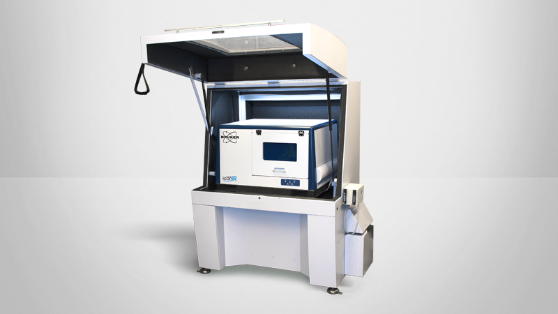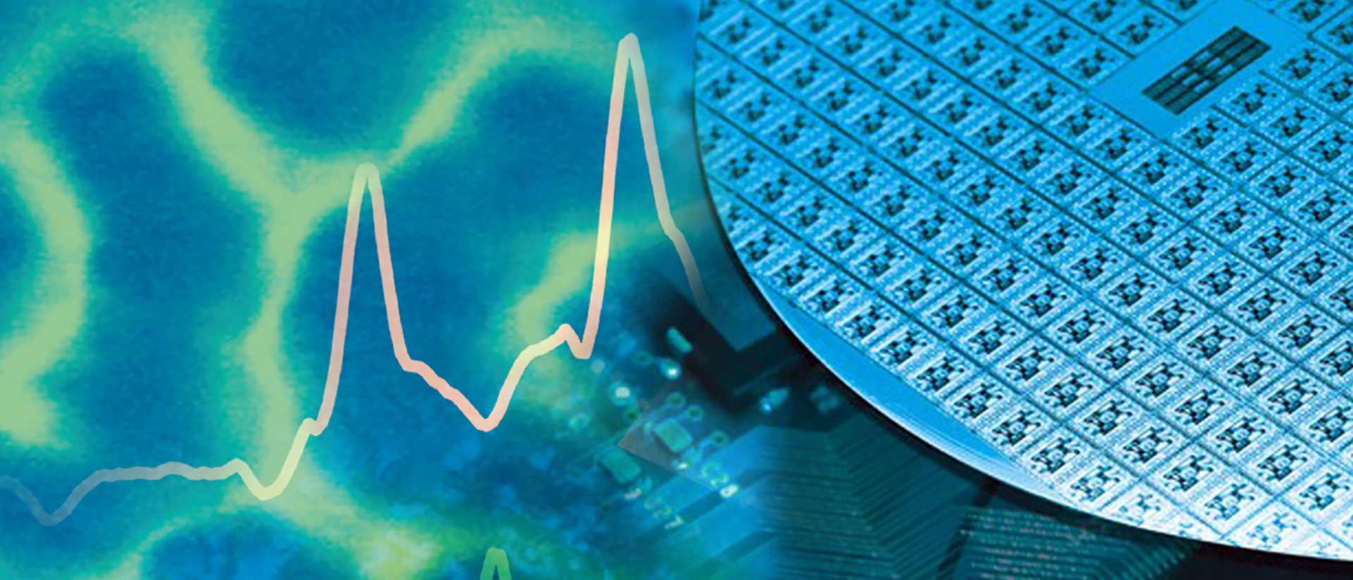

Large-Sample Dimension IconIR300: Defect Detection and Chemical-ID Characterization of Semiconductor Devices
Innovative IconIR technology creates new research opportunities for semiconductor researchers and engineers.
This workshop focuses on the capabilities of the large-sample Dimension IconIR for semiconductor and microelectronic devices, full-size wafers and photomasks, and interconnect devices. Topics include defect detection, chemical identification of nano-contaminants, and material property mapping.
Explore Large-Sample NanoIR for Semiconductor Industry Applications
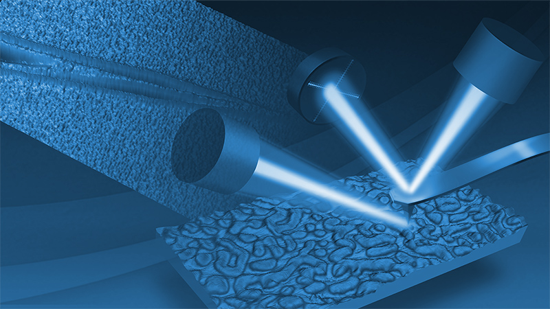
This virtual workshop focuses on defect detection and the chemical-ID characterization of semiconductor and microelectronic devices using photothermal AFM-IR spectroscopy and imaging.
Our applications experts will discuss and demonstrate the use of the new IconIR system for
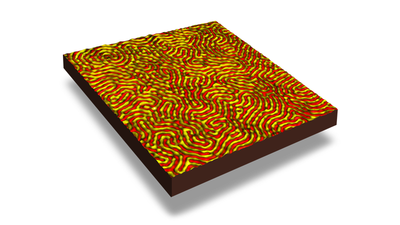
- Characterization of nm-features in semiconductor and microelectronics devices;
- Chemical identification of organic contaminants on full sized wafers or photomasks; and
- Chemical characterization of nano-patterned metal/low-k dielectrics used in advanced micro/nano-fabrications.
This recording also includes a Q&A session with the presenters, during which they respond to questions posed by researchers in the semiconductor industry. Topics covered include available configuration options, recommended tip selection for semiconductor applications, and system stability and drift rates.
Find out more about the technology featured in this webinar or our other solutions for semiconductor research:
Sections
| Length | Topic | Title |
|---|---|---|
| 10 Minutes | An Introduction to the Dimension IconIR | AFM Meets Infrared: Photothermal AFM-IR Spectroscopy and Imaging |
| 15 Minutes | Applications in the Semiconductor Industry | From Defect Detection to Chemical Identification of Nano-Contaminants |
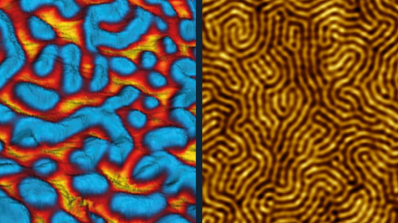
| 15 Minutes | Demonstration of the Dimension IconIR | Chemical Identification and Material Property Mapping of Wafers and Interconnect Devices |
| 15 Minutes | Live Q&A with the Speakers |