Crystalline Defects in Si Substrates
X-ray Diffraction Imaging
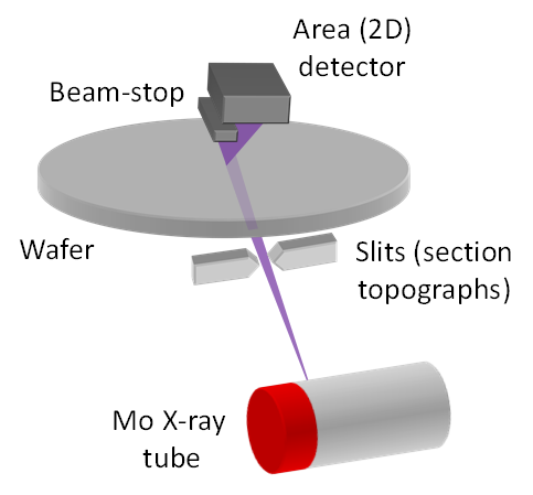
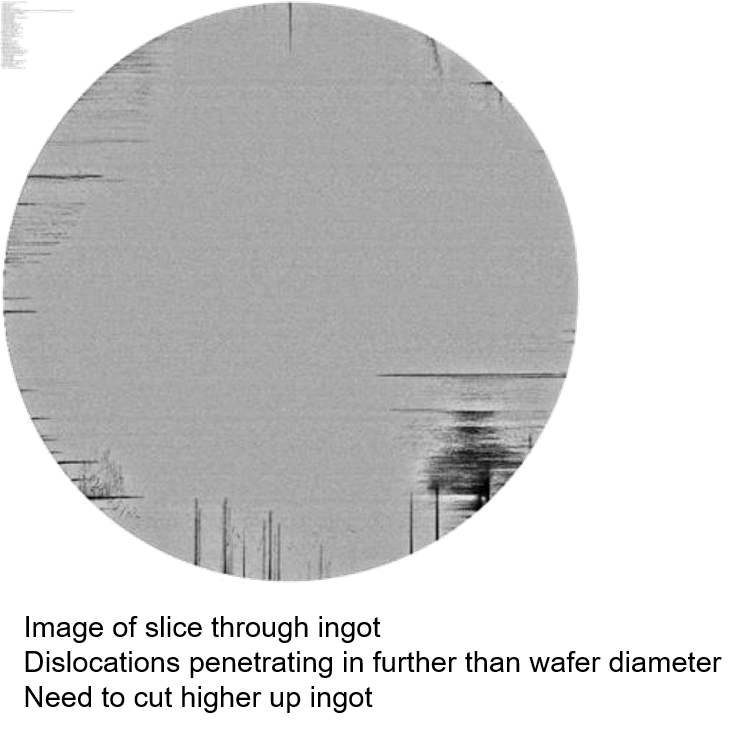
X-ray diffraction imaging (XRDI, also known as X-ray topography) is used to image crystalline defects in otherwise perfect (or near perfect) substrates. In Si substrate manufacture, imaging of an ingot slide without sample preparation, even before mirror etching or directly after grinding, is performed. The defect map from the ingot can indicate the location on the boule to start slicing for good wafers. As no sample etch is required, this reduces the amount of harmful etch acids used in the production environment.
Instantaneous Feedback To Production
XRDI can also be used to identify any cracks or slip on the wafer edge after processing, and the addition of a mini-environment and edge grip sample handling allows final quality checks on product to be performed.
The fully automated nature of the QCTT tool allows the defect maps to be extracted and automatically reported via SECS/GEM for instantaneous feedback to production.
Micro-XRF
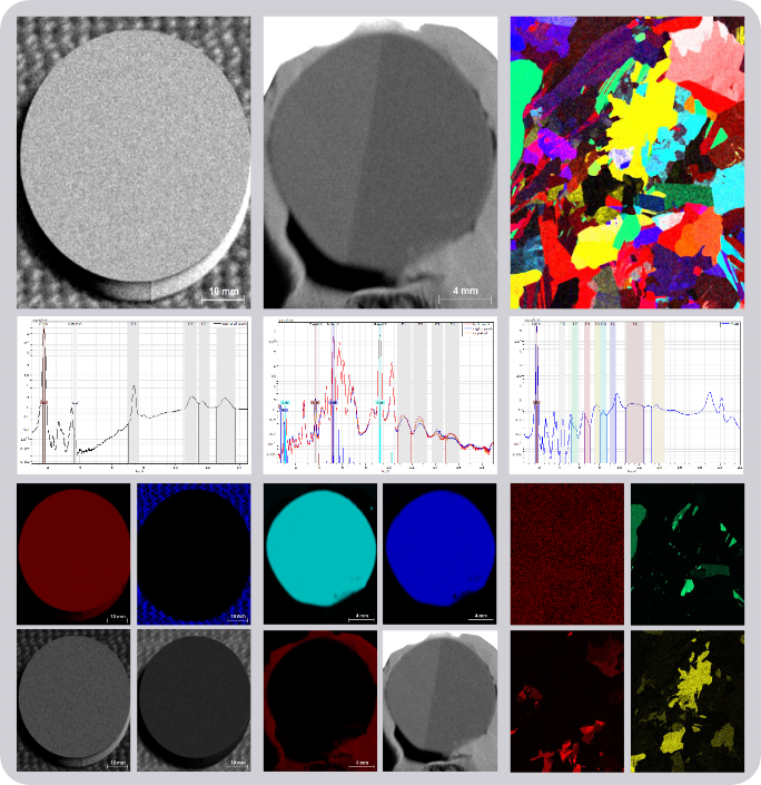
In large crystals, most defects come with a change in lattice constants and / or change in the crystal orientation. Those changes will result in a variation in the Bragg peaks in the micro-XRF spectrum. They can be mapped over large areas thanks to Bruker's micro-XRF solutions.
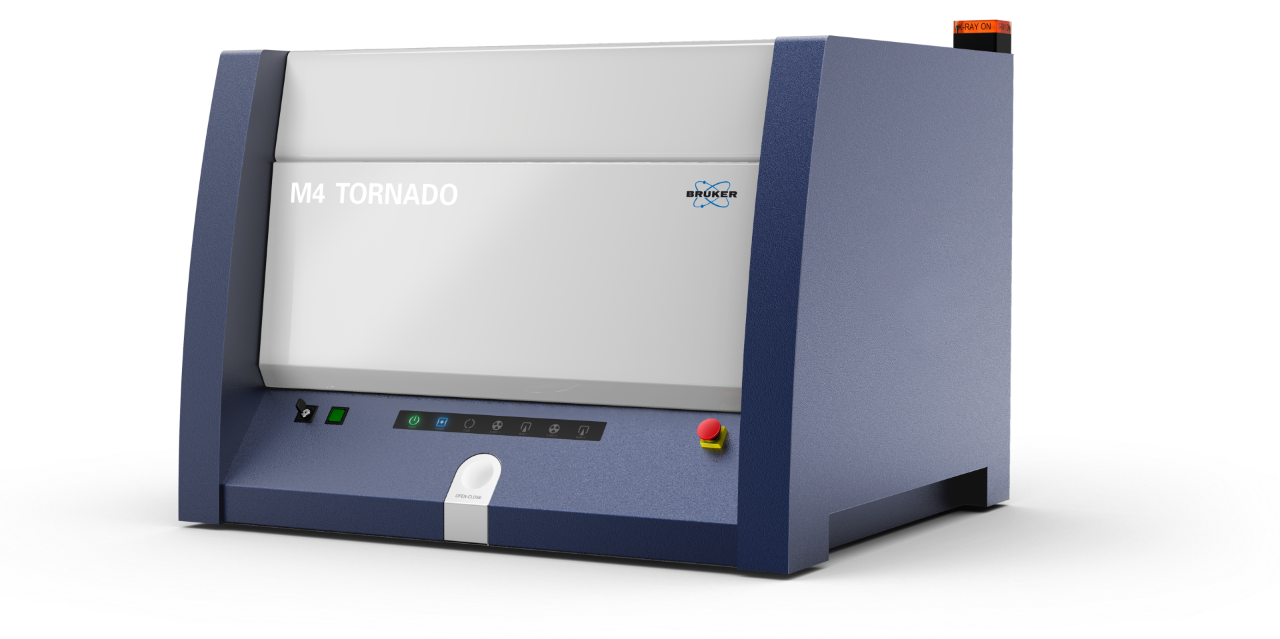
Fast Crystal Domain Mapping Using Energy-dispersive micro-XRF
In energy-dispersive XRF, Bragg diffraction peaks are often considered a bothersome artifact interfering with the fluorescence information. However, these Bragg peaks, as they are related to crystal orientation, provide additional information on the nature of the sample. Here, we describe how the M4 TORNADO can be utilized to visualize crystal domains. This information is crucial to evaluate the quality of single crystals as well as the properties of polycrystalline materials. This principle can be used to identify sub-grain misorientation in single crystals as well as crystallite dimensions within multi-crystalline samples.
Read also this related publication: