Superconductors & Metal Composites
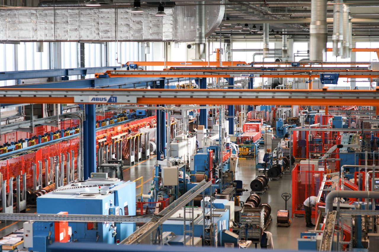
Bruker Energy & Supercon Technologies (BEST)
Welcome to BEST, a leading manufacturer and developer of high-performance superconductor wire products and research instrumentation. At BEST, it is our mission to use our unique knowledge in advanced materials and devices to provide the world with better, cleaner solutions that lower the impact on the environment and help improve lives.
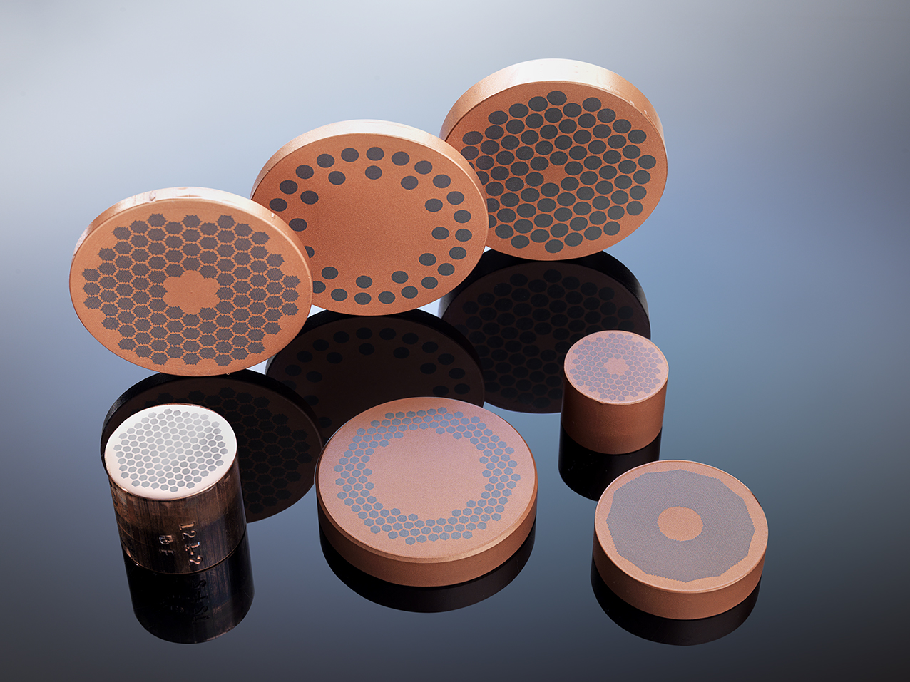
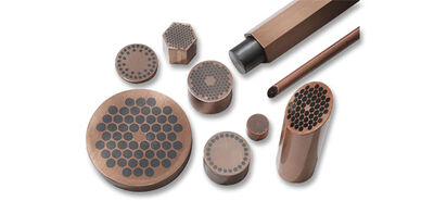
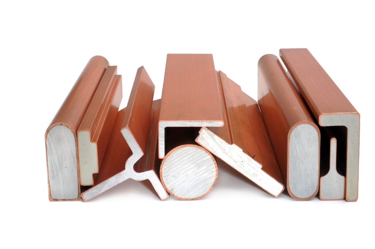
With more than 50 years of experience in superconductors and more than 40 years of experience in Cuponal copper aluminum composites as well as over 15 years in research instrumentation, BEST provides a unique spectrum of technologies to meet the demands of fast growing markets in healthcare, energy and research. Our highly motivated and interdisciplinary teams provide high-tech solutions for today's customers while working on new ideas for tomorrow's challenges.