PCBs and Consumer Electronics
Root Cause Particle Analysis Using a Particle Trap and FT-IR Microscopy
No matter whether one speaks of fine dust or microplastics. Tiny particles are everywhere and apart from their impact on human health, they are one of the main causes of product damages and defects during production.
Wherever technical cleanliness is the be-all and end-all, a reliable residual dirt analysis is also a must. FT-IR microscopy is a vital tool for tracking contamination routes and identifying the root cause.
In cooperation with other tools such as particle traps, entire spectral libraries of potential particle causes can be created. These can be searched in the event of defects and failures, to immediately clarify the reason for the damage.
Contamination and Failure Analysis of a PCB by FT-IR Microscopy
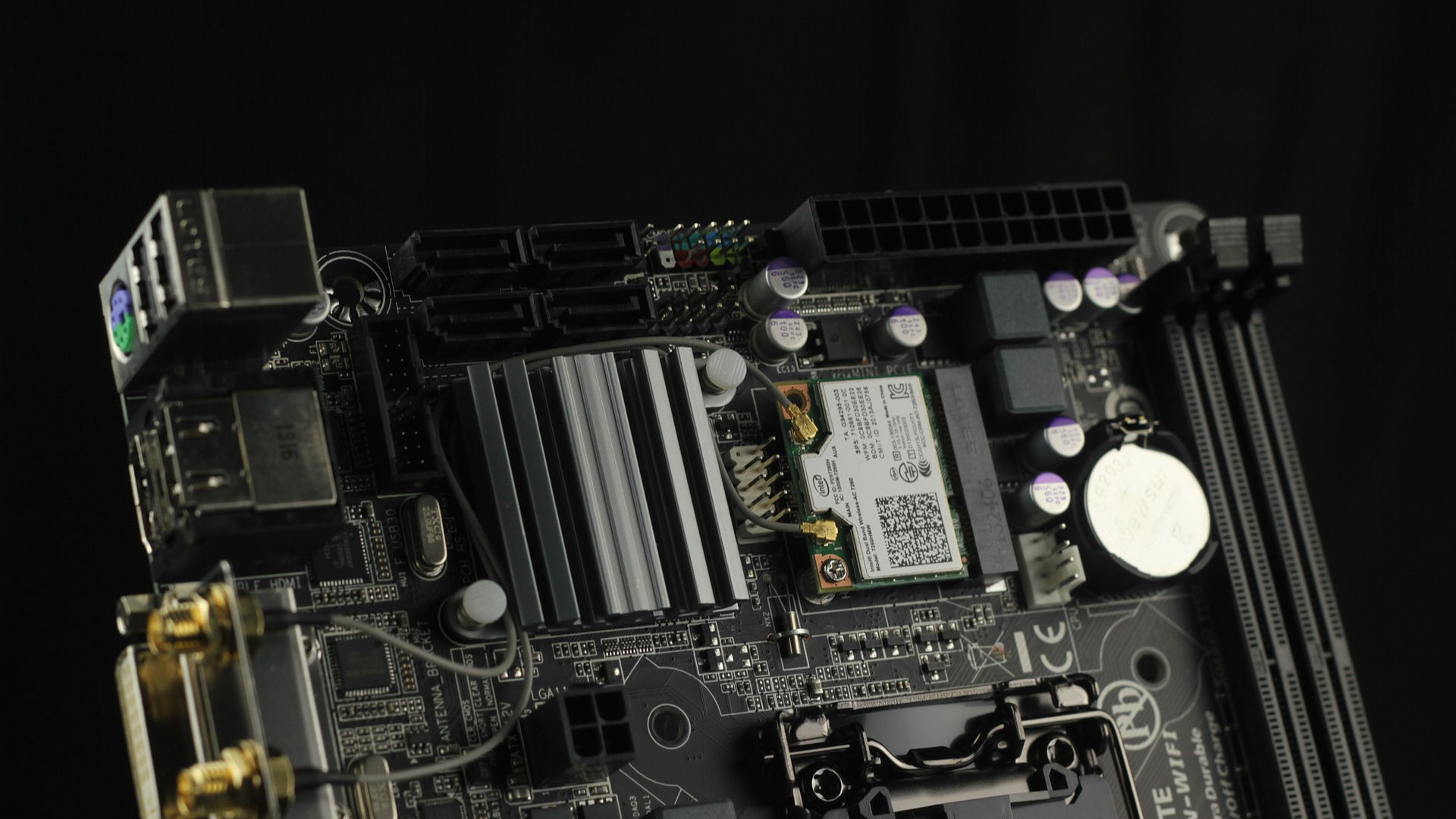
A PCB failure is typically linked either to damage caused by the PCB manufacturer during production, transport or due to environmental stresses. If such a failure occurs is often costs a lot of time and nerves.
In order to save both of these valuable resources, FT-IR microscopy is a good choice, since it can contribute significantly towards understanding when and how a PCB damage occurred. Through careful microscopic chemical analysis, FT-IR microspectroscopy supports you in the following applications:
- Customer complaints
- Process troubleshooting
- Product failure and defect analysis
Analysis of a CMOS Chip Circuit Board by FT-IR Microscopy
Contaminations have a negative impact on the product quality; especially in the field of microelectronics impurities are an extremely important topic. Revealing the contamination's origin and enabling quick troubleshooting is one of the key advantages of FT-IR microscopy.
One huge advantage of infrared spectroscopy is the chemical contrast it offers to a simple visual inspection. This means, that even contaminations that are undetectable have remained undetected first, can be discovered by using FT-IR spectroscopic methods.
It is traditionally used to identify soldering and washing residues, damaged contacts, damaged resistors or in any kind of Residual dirt analysis

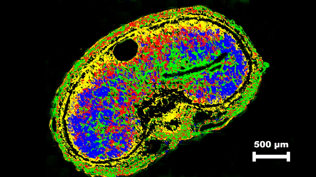
Elemental Distribution Analysis of Electronic Components with micro-XRF

Microelectronic components are of increasing complexity. The size and distances of the surface mounted devices (SMD) and integrated circuits (ICs) are getting smaller and the wires and connections are implemented in several layers within the printed circuit board (PCB). Therefore, analytical methods to approach these sort of samples need both, a high spatial resolution and the capability to look into the depth of the sample.
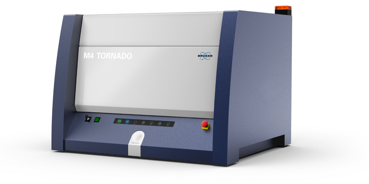
Micro-XRF is an imaging technique which combines spatial resolution of roughly 20 µm with a very high elemental sensitivity for most metals. The M4 TORNADO can therefore be a companion in the complete life cycle of electronic components, from R&D for novel designs and materials to recycling of precious metal components.
A new Dimension for Failure Analysis
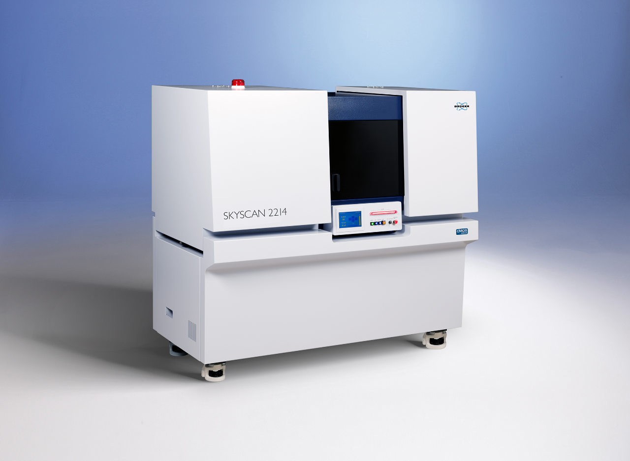
Consumer electronics contain a myriad of devices and sensors. As time goes on, the number of these components has increased exponentially while being placed in an ever-shrinking external package. X-ray Microscopy allow the non-destructing imaging of these items without the need for disassembly. This also presents an opportunity for next generation repair as failure mode can be diagnosed without having to open the case, a time-consuming process which often involves adhesives and specialty tools.
Fast, Non-destructive Quality Control of Electroless Nickel Coatings with micro-XRF

Electroless nickel plating (ENP) is an auto-catalytic chemical process used to deposit a layer of nickel-phosphorus (Ni-P) alloy coating on a substrate. The nickel-phosphorus coating thickness varies typically from 1 to 40 μm depending on the application. Electroless nickel coatings can have varying phosphorus content which impacts specific metallurgical properties. The phosphorus range typically varies from 2% up to 15% level. One of the key benefits of the nickel-phosphorus coating is that it provides a very consistent thickness that isn't dependent on part geometry. Electroless nickel plating can reach all hidden surfaces to offer complete coating coverage even on the most intricate parts. Electroless nickel coating is used for example in printed circuit boards and connectors.
When tight quality control of metal coatings is required, X-ray fluorescence (XRF) analysis is the best overall solution. The modern micro-XRF instrument, such as the Bruker M4 TORNADO can provide simultaneous coating thickness and coating composition measurement.
Restricted Material Screening with micro-XRF
With the increasing presence of electronic devices, electronic waste is also being produced faster than ever before. In recent years the EU and other countries have established multiple regulations to promote recycling of e-waste and reduce the health and environmental risks associated with the increase in e-waste production. RoHS directive (Restriction of the use of certain Hazardous Substances) is one of those rule sets aimed at reducing hazardous material from entering e-waste streams by restricting their use in electronic equipment. These restricted materials include heavy metals (lead, mercury, cadmium), hexavalent chrome, polybrominated flame retardants (PBB and PBDE) and phthalates.
X-ray fluorescence (XRF) offers a fast, non-destructive method of screening for these restricted elements. Small spot analysis is important for successful analysis, since the analysis beam must match the sample size which makes M4 TORNADO micro-XRF perfect choice for RoHS screening. For RoHS screening selectable collimator between 0.4 mm and 1.5 mm allows accurate analysis on individual components and cables, as well as bulk samples (metals, solder, raw materials) and large circuit boards.

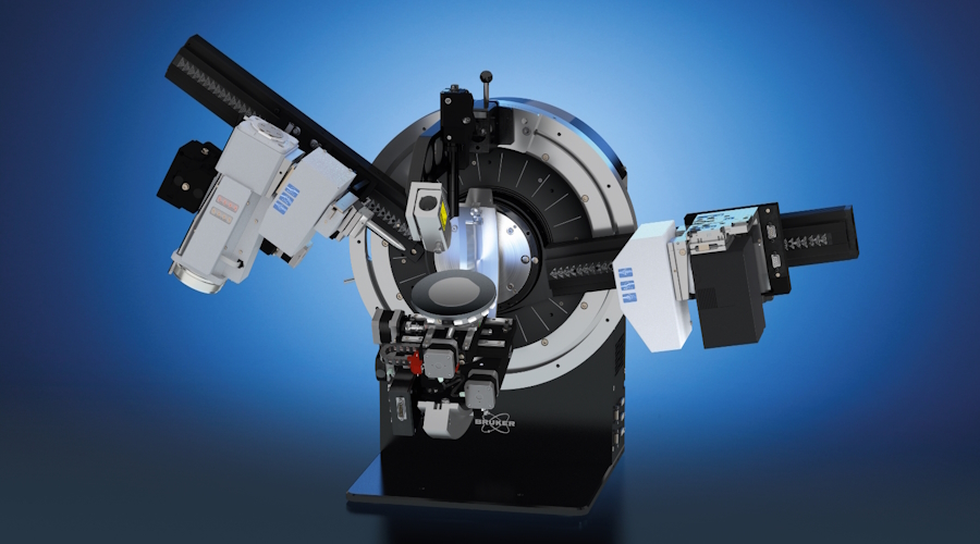
Analysis of Soldered Joints with XRD

Electronic components are electrically and mechanically fixed to circuit boards with solder. The interaction of environment, flux and solder can lead to a myriad of crystallographic phases with differing properties. XRD goes beyond routine elemental analysis by positively identifying the phases that are present enabling proper diagnosis of failure mode.