
Experience our Breakthrough Electron Microscope Detectors
Redefining Elemental and Nanostructural Analysis on the SEM
Be one of the first to discover Bruker's two new groundbreaking detector technologies, which are set to redefine analysis on the SEM:
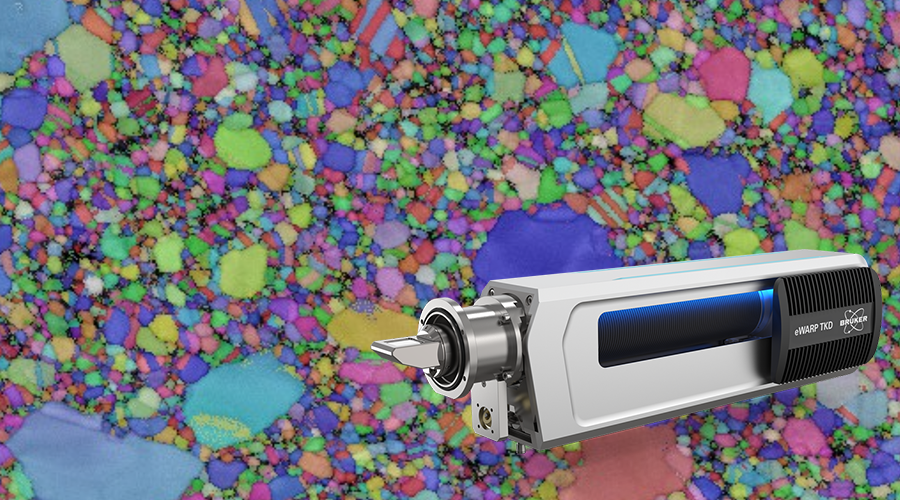
eEWARP TKD: a next-generation on-axis Transmission Kikuchi Diffraction (TKD) detector for nanostructural analysis.
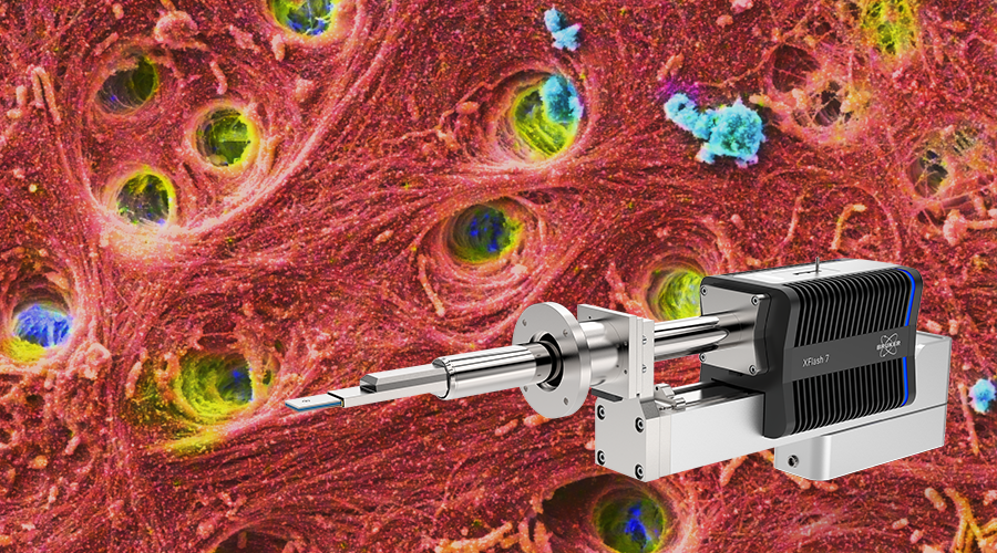
XFlash FlatQUAD 2L: our annular EDS detector for maximized collection efficiency, now with parallel BSE imaging.
Continue reading to learn more about how this breakthrough detector technology will revolutionize your research, the conferences where they will be showcased, or to sign up for the launch webinars.
eWARP TKD: Ultra-Fast High-Resolution Nanomaterials Characterization
Powered by Bruker's innovative WARP sensor technology, eWARP TKD is a dedicated on-axis Transmission Kikuchi Diffraction detector designed for nanomaterials characterization in the SEM.
Featuring a newly developed pixelated sensor with 162 × 162 pixels and an active area exceeding 26 × 26 mm², eWARP TKD combines exceptional sensitivity with ultra-fast acquisition speeds of up to 5,700 fps.
With better than 2 nm spatial resolution, integrated Dark Field and Bright Field imaging, and an on-axis geometry, eWARP TKD redefines what is possible in TKD analysis.

Unmatched TKD Performance
Characterize nanomaterials with spatial resolutions better than 2 nm.
Acquire high-quality orientation and phase maps in 1–5 minutes at speeds of up to 5,700 fps.
Capture real-time microstructural evolution during in-situ heating and mechanical testing.
Perform low-dose TKD analysis on beam-sensitive and delicate materials.
Minimize drift-induced artifacts through ultra-fast mapping and reduced acquisition times.
Collect Bright Field and Dark Field images simultaneously alongside TKD data.

Discover XFlash® FlatQUAD 2L: Maximum Efficiency in X-ray Collection
Featuring four silicon drift detector (SDD) segments with 100mm2 area arranged around a central aperture, XFlash® FlatQUAD 2L combines exceptional X-ray collection efficiency with true parallel EDS and BSE acquisition.
With solid angles exceeding 1 sr, count rates up to 8 million cps ICR (input count rate), 4 million cps OCR (output count rate) and energy resolution down to 127 eV at Mn Kα: XFlash® FlatQUAD 2L is designed to support both routine analysis and challenging applications.

One Detector. Any Application.
Perform SEM EDS at ultra-high spatial resolution, enabling analysis of nanostructured materials and semiconductor devices.
Quantify elemental compositions at high throughput with exceptional count rates and collection efficiency.
Overlay X-ray EDS data with true parallel BSE images for correlated chemical and compositional information.
Analyze delicate, beam-sensitive, or charging samples with low kV, low beam currents, low vacuum conditions.
Accurately map the elemental composition of rough and topographic samples where conventional detector geometries are limiting.
Perform TEM-like EDS analysis using a SEM, enabling elemental characterization of electron-transparent specimens using STEM-in-SEM workflows.


See the Detectors in Action: Visit Bruker at a Show
Bruker will be attending the following shows with live demos.
- M&M: Microscopy & Microanalysis - 2nd to 6th August - Milkaukee, WI, USA.
- IMC: The International Microscopy Congress - 31st August to 4th September - Liverpool, UK.
Get in touch with your local Bruker representative to book a demo now.
Ready to Learn More? Register for the Launch Webinars
Contact a Bruker Expert
If you would like to know more about how our new, industry-leading detector technology can accelerate and level up your SEM-based analyses contact a Bruker expert.