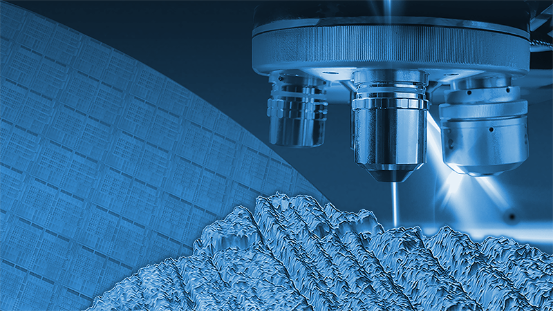
WLI Measurement Modes
Bruker’s primary white-light interferometry (WLI) modes are phase shifting interferometry, vertical scanning interferometry, and universal scanning interferometry. These acquisition modes have different strengths, and selecting the appropriate mode is essential to ensure accurate, repeatable results.
Phase-Shifting Interferometry (PSI)
PSI is the highest-resolution mode, designed for ultrasmooth reflective surfaces. It operates by introducing controlled phase shifts in the reference beam and capturing a series of interferograms. These phase-shifted images are then processed to reconstruct the surface topography with sub-angstrom vertical resolution. PSI is ideal for applications where nanometer-scale surface quality is critical, such as optical flats, mirrors, and semiconductor wafers.
Vertical Scanning Interferometry (VSI)
VSI is a scanning mode that captures a stack of interferograms while vertically translating the objective through the focus range. It is suitable for surfaces with moderate to high roughness and varying reflectivity. VSI is widely used in semiconductor packaging, MEMS, and precision machining applications.
Universal Scanning Interferometry (USI)
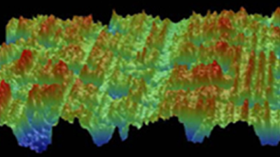
USI is a hybrid mode that combines the strengths of PSI and VSI. It employs adaptive algorithms to analyze each pixel individually, selecting the optimal processing method based on local signal characteristics. This enables accurate measurement of surfaces with mixed topographies, such as smooth regions located next to rough features.

Frequently Asked Questions about WLI Technology
Bruker offers phase shifting interferometry (PSI), vertical scanning interferometry (VSI), and universal scanning interferometry (USI) modes.
PSI is designed for very smooth surfaces and small step heights, VSI is optimized for rough surfaces and large vertical steps, and USI automatically adapts signal processing to the surface type to capture accurate topography across mixed textures in a single measurement.
PSI is used for smooth surfaces (roughness less than 30 nm) and small steps, such as mirrors, optical flats, and semiconductor wafers. It has ultrahigh, sub-nanometer resolution for vertical measurements.
VSI is suitable for surfaces with moderate to high roughness and structures with larger height variations. It is compatible with surfaces of varying reflectivity, and is widely used in semiconductor packaging, MEMS, and precision machining applications.
USI is ideal for the measurement of any surface, from smooth, rough, steps, or a combination of surfaces in one image. It employs adaptive algorithms to analyze each pixel individually, selecting the optimal processing method based on local signal characteristics. USI produces fast, accurate results capable of providing striking details for a huge range of applications.
The AcuityXR® measurement methodology can also be used with USI for the absolute highest lateral resolution available for a given magnification and field-of-view combination.