InSight 300
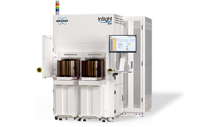
InSight 300
InSight 300 is a fab-ready automated atomic force microscope (AAFM) designed for reliable, cost-effective inline metrology in high-volume semiconductor manufacturing environments. With <±1nm scanner flatness and a best-in-class noise floor of <35pm, this system meets the rigorous requirements of advanced CMP and etch applications, from micron-roughness to fully automated bare-wafer defect review. Its profilometry capabilities meet and exceed the millimeter-scale and bevel-edge metrology requirements for cutting-edge hybrid bonding applications. InSight 300 also features Bruker-proprietary operating modes for optimized measurements of sidewall roughness, automatic bare-wafer defect review, and advanced profiling of feature surfaces.
High-Throughput AFM for Accurate Inline Measurements

InSight 300 leverages Bruker’s two and a half decades of experience developing AFM innovations that improve resolution, stability, versatility, and ease of use. Its exceptionally high throughput, accuracy, and reliability ensure trustworthy results at a low total cost of ownership.
InSight 300 features:
Built with Semiconductor Metrology Expertise
Experience, Service, & Support
Bruker automated atomic force microscopes (AAFMs) are a long-trusted solution for semiconductor fabs worldwide. From the first fully automated 200mm fab AFM to the latest InSight 300, Bruker has introduced patented AAFM innovations that have enabled continual development of next-generation semiconductor devices.
We are dedicated to keeping your tool running at the peak of up-time and productivity. Bruker provides:
- A worldwide service and support team that excels in first-time solution of issues.
- Strategically placed service depots to ensure part availability.
- A variety of service coverage programs to match your specific support requirements.

Specialized Probes
Application-dedicated probes provide the most reliable, accurate characterization of advanced nodes. Bruker is the only AFM manufacturer that also owns and operates a probes nanofabrication facility, where we continually develop novel probe designs optimized for specific applications.

Focused on Production
Superior Capabilities
InSight 300 delivers stable, NIST-traceable, artifact-free data. It integrates built-in expertise to perform accurate and repeatable:

Application-Specific Modes
Operating modes dedicated to specific applications can obtain the highest metrology accuracy while maximizing throughput. InSight 300 offers Bruker’s patented operating modes purpose-built for roughness (TrueSense®), sidewall roughness and angle (CDMode), depth of high aspect ratio features (DTMode), and surface profiling.

Automatic Tip Management
Bruker’s TipX technology on InSight 300 provides true probe automation and full confidence in quality for HVM. Probes are automatically loaded and qualified, ensuring each meets recipe requirements. Probes are held reliably by vacuum, providing maximum flexibility for probe selection and reducing the cost of probes.

Verified Performance
During our development and production processes, performance is continuously verified and confirmed by long-term stability, linearity, and accuracy tests. With less than ±1nm of out-of-plane motion over the full 105µm2 scan range and up to 18µm of Z range, and the addition of a long-range profiling stage, InSight 300’s AFM scanner with a scanning-tip design is optimized to handle modern nanoscale metrology challenges.

Versatile Optics
InSight 300’s integrated optics enable easy navigation to areas of interest and time-efficient creation of recipe sites. A combined dual-channel, tip-centric objective and third offset objective provide unrivaled optical resolution while maintaining maximum FOV.

Modern GUI
Ease of use is designed into InSight 300. An operator-friendly GUI enables rapid, good recipe generation by technicians and engineers, including recipe-controlled tip management and resource tracking. Recipes can be generated and modified off-tool to keep tools in production during development.

Optimized for Your Applications

Roughness Metrology
InSight 300's best-in-class noise levels enable sub-angstrom surface roughness control, with quantitative roughness measurements below 100pm RMS. Even at MAM times of ~1 min/site, roughness data is accurate and reliable, with excellent repeatability (e.g. 3σ<10pm for smooth surfaces with RMS roughness <1nm) and tip-to-tip reproducibility.
Image: (left) Ultrasmooth Si (85pm RMS, 1nm Z scale, 1x1µm scan). (middle) Post-CMP ILD area with 0.42nm RMS (8nm Z scale, 3x3µm scan). (right) High-throughput roughness metrology repeatability result on two Si wafers with 106pm RMS and 83pm RMS, 3σ<5pm. Acquired at <1 min MAM time.

Depth Metrology
Deep trench mode (DTMode) is Bruker’s proprietary AFM mode developed specifically for narrow trenches and vias with depths from 10s of nm to over 10µm. With a <10s MAM time, DTMode in combination with application-dedicated high aspect ratio tips meets the depth metrology requirements for HVM etch process control.
Image: (left) DTMode scan and (right) section profiles of a dense array of vias (depths 80 to 100nm), enabling within-wafer process variation studies.

Sidewall Profiling
Sidewall angle (SWA) and sidewall roughness (SWR) are critical metrics for device and IC performance. Measuring these critical dimensions with AFM can only be performed with a mode truly designed for this metrology; tilting a scanner introduces significant TMU. Bruker’s critical dimension scan mode (CDMode) is the world's only true CD-AFM metrology with unparalleled accuracy, unmatched repeatability, and the industry’s proven lowest TMU.
Image: (left) CDMode characterizes a line/space pattern with 150nm pitch for (middle) high-resolution SWA, and (right) line edge roughness.

Automatic Defect Review
AFM defect review is a non-destructive alternative to traditional review techniques (e.g., SEM/EDX) that also uniquely measures adhesion, further aiding with defect classification. InSight 300 defect review can be fully automated and recipe-driven, with KLARF compatibility. Maximum productivity is achieved through rapid recipe creation in under five minutes and automated bare wafer registration, reaching throughputs of tens of defects per hour.
Image: High-resolution height scans of various nanometer-scale defects (2x2µm scans), and simultaneously acquired adhesion measurements (final two images, in pink) further aiding defect classification.

Surface Profiling
InSight 300 can be configured to include best-in-class profiling. Measurements can cover up to a 50mm distance at speeds up to 1mm/s, enabled by state-of-the-art non-contact linear stage motion with focus on both local and long-range planarity. Profiling applications include post-CMP characterization of dishing and erosion, bevel edge rounding, and step height measurements.
Image: Post-CMP profiling (2nm data spacing) with high repeatability for both dishing (3σ = 0.14nm) and erosion metrology (3σ = 0.32nm).

Hybrid Bonding
The Insight 300 automated AFM can be applied in the most current hybrid bonding technology nodes providing high resolution imaging and dedicated analysis for critical bond pad metrology as well as automated bevel edge metrology for hybrid bonding.
Image: Cu/ILD pattern post CMP revealing critical roughness and recess depth information for the hybrid bonding process.
Contact us to discuss your specific application, process needs, and measurement requirements.
InSight 300 Automation Specifications
Each wafer manufacturing facility and semiconductor fab has its own specific requirements and challenges. Our listed product specifications and offerings are always a starting point for a conversation with our experts to determine how our capabilities can meet your needs.
| Fab Automation | SECS/GEM Host Automation Interface, E84 PI/O AMHS support |
| SEMI Standards E4, E5, E30, E37 & E37.1, E39 & E39.1, E40, E87 & E87.1, E90, E94, E116 & E116.1 | |
| Regulatory Compliance: CE, UKCA, KC, SEMI S2/S8, F47, 21 CFR 1040.10, 21 CFR 1020.40 | |
| Tip Handling | Automated Tip Management and Tip Exchange |
| Tip Capacity: 4 Cassettes, 25 Tips each |
How Can We Help?

How Can We Help?
Bruker partners with our customers to solve real-world application issues. We develop next-generation technologies and help customers select the right system and accessories. This partnership continues through training and extended service, long after the tools are sold.
Our highly trained team of support engineers, application scientists and subject-matter experts are wholly dedicated to maximizing your productivity with system service and upgrades, as well as application support and training.