nanoECR
Conductive Nanoindentation
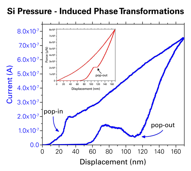
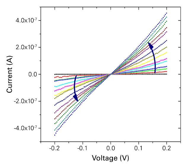
The combination of electrical contact resistance measurements with nanoindentation provides valuable new insights into contact resistance evolution and material deformation behavior at the nanoscale. By passing current through a conductive nanoindenter probe, nanoscale electrical characteristics can be determined as a function of applied probe force and probe displacement into the sample surface. In addition to quantitative measurement of I-V characteristics of nanoscale electrical contacts, new insights can be gained in the areas of thin film fracture, dislocation nucleation, deformation transients, contact resistance, fatigue, diode behavior, tunneling effects, piezoelectric response, phase transformations, and more.
In-Situ Electrical and Nanoindentation Measurements
Bruker’s nanoECR utilizes a new model of Bruker’s proprietary electrostatic transducer that has been modified to provide an electrical path from a sample biasing stage through a conductive indenter probe to enable a continuous measurement of evolving electrical contact conditions as a function of applied force and probe displacement. Operating under feedback control, nanoECR enables constant voltage or I-V sweep measurements from nanoscale probe contacts during highly controlled applied load or probe displacement conditions.