GaN on Si Power Device Metrology
GaN on Si Power Device Metrology
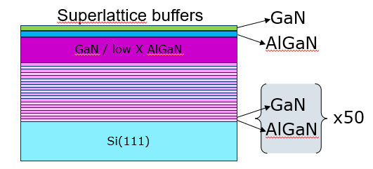
GaN on Si power devices can be grown of both stepped and superlative buffers, but the device layers are the same for both types.
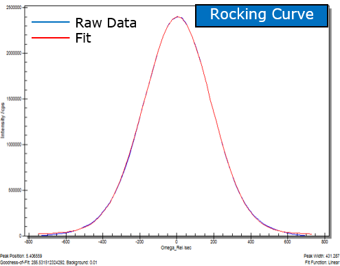
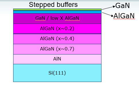
Stepped buffers are used for low voltage devices and are generally less complex structures. In these buffers, the composition of individual layers is required and can be obtained from HRXRD measurements along with the quality obtained from the width of the rocking curves.
Superlattice buffers are more complex and have been developed for higher voltage devices. They consist of repeated bilayers of AlGaN / GaN (or similar) layers and HRXRD provides the superlattice period and average AlGaN composition in the superlattice.
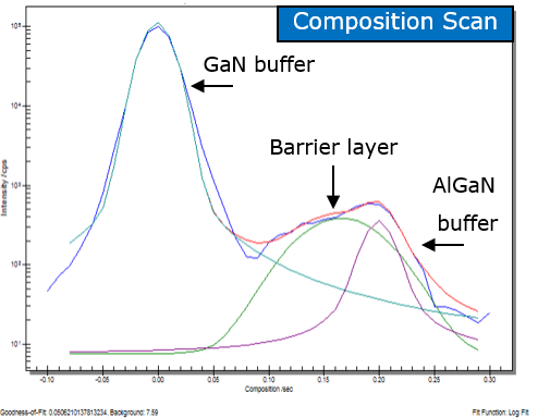
Irrespective of the buffer layer, the device layer parameters required from X-ray measurements are the thickness of each layer and composition of AlGaN barrier layer. These can be found from a combination of X-ray scans.
Full Suite of Metrology
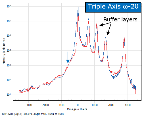
A full suite of metrology has been developed for GaN on Si applications. These include using triple axis scans for buffer layer analysis, rocking curves for quality and combinations of ultra-fast RSMs (down to 10 seconds) and composition scans for full characterization of the structure.