
A New Frontier for Nanomaterials Research in SEM
Meet eWARP TKD: The Key to Ultra-Fast High-Resolution Nanomaterial Characterization
Watch this webinar to discover eWARP TKD.
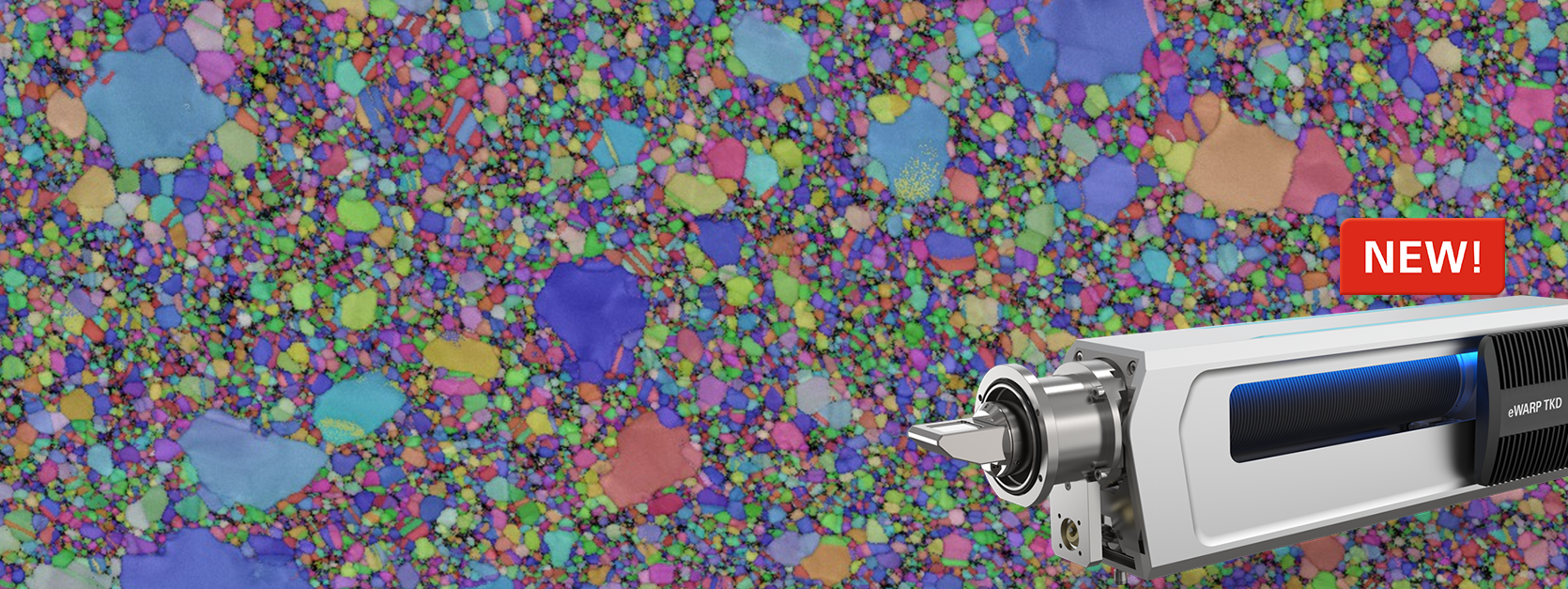
eWARP TKD is purpose-built for nanomaterials characterization in the SEM. Built with an on-axis TKD geometry and equipped with our industry-leading Wide ARea Pixelated (WARP) technology, eWARP TKD sets a new benchmark for sensitivity, speed, spatial resolution, and data integrity.
In this webinar, we will introduce the technology behind eWARP TKD and demonstrate how its exceptional signal efficiency and acquisition speeds of up to 5,700 fps enable high-quality orientation and phase mapping in just minutes.
Attendees will discover how eWARP TKD delivers sub-2 nm spatial resolution, ultrafast DF and BF-like imaging, artifact-free mapping with minimal beam requirements, and new opportunities for time-resolved in-situ experiments and the characterization of beam-sensitive materials.
What to Expect
The webinar will feature a variety of application examples spanning advanced nanomaterials research, showcasing how eWARP TKD is accelerating discovery while expanding the capabilities of SEM-based electron diffraction.
Whether you are studying semiconductors, energy materials, nanostructured metals, or other emerging materials, this webinar will provide insight into the next generation of TKD performance.
Speakers

Dr. Daniel Goran
Product Manager EBSD, Bruker Electron Microscope Analyzers

Dr. Yang Yang
Application Scientist, Bruker Electron Microscope Analyzers