eWARP TKD: Ultra-Fast & High-Resolution Transmission Kikuchi Diffraction
Best Spatial Resolution. Maximum Throughput. Zero Compromise.
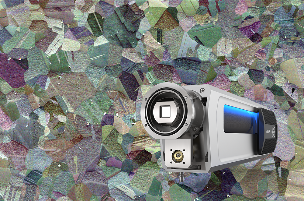
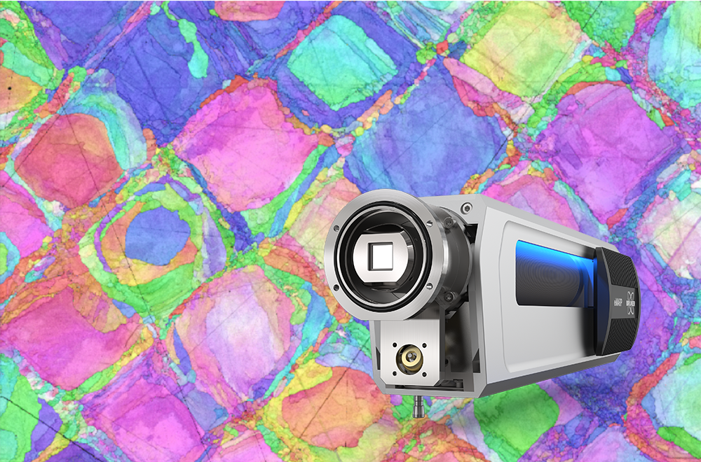
eWARP TKD is the latest addition to the award-winning eWARP family of detectors, powered by Bruker’s cutting-edge Wide ARea Pixelated (WARP) sensor technology, and designed specifically for Transmission Kikuchi Diffraction (TKD).
With eWARP our unique WARP sensors began a new era of EBSD with ultra-fast mapping speeds at unprecedented spatial resolution and more. Leveraging the same breakthrough WARP technology, eWARP TKD is redefining the limits of TKD (also known as Transmission EBSD), opening new possibilities for high-resolution nanomaterial analysis.
At the core of the system is a newly developed pixelated sensor with 162 × 162 pixels and an active area exceeding 26 × 26 mm2.
eWARP TKD is purpose-built for nanomaterials characterization using the "on-axis" sample-detector geometry in the Scanning Electron Microscope (SEM). eWARP TKD outperforms existing solutions across all key metrics, with unmatched sensitivity, speed, spatial resolution and data integrity.
eWARP TKD is a detector for our QUANTAX EBSD analytical system.

Take Nanomaterials Characterization to the Next Level with eWARP TKD
eWARP TKD redefines nanomaterials characterization in the SEM, delivering a powerful set of advantages for researchers and engineers working on nanomaterials:
- Massive productivity gains: eWARP TKD delivers high-quality orientation and phase maps within 1-5 minutes at speeds of up to 5,700 fps
- Unmatched spatial resolution: Combined with a high-end FE-SEM, eWARP TKD delivers mapping at better than 2 nm spatial resolution.
- Integrated Dark Field (DF) and Bright Field (BF) imaging at lightning speed: Enabled by eWARP’s patented on-chip binning technology.
- Time resolved mapping during in-situ experiments: Rapidly acquire maps and images every few seconds to capture real-time microstructural evolution in electron-transparent samples during in-situ heating and mechanical testing.
- No drift correction. Minimal artifacts: Thanks to low beam requirements and ultrafast mapping, eWARP TKD renders drift correction obsolete and produces maps with minimal drift induced artifacts.
- Engineered for delicate samples: Extreme signal efficiency enables low-dose, low-kV TKD mapping for beam-sensitive materials.

Unmatched Performance for the Characterization of Nanomaterials
Figure 1 depicts a very large orientation map (IPFz) acquired with 2 nm steps from a 15nm Gold thin film (planar view). The inserts show the equivalent grain diameter size distribution of all grains smaller than 50 nm (top left) and a zoomed-in view of the highlighted area (top-right).
Please note that no data cleaning was applied and that crystals made of less than 5 pixels were excluded from the histogram and statistics (see cutout in data around 5 nm).
- Map size: 4.3 Mpixels / 5.1 µm x 3.9 µm
- Pixel size: 2 nm
- Indexing rate: 92.5%
- Speed: 2873 patterns/second
- Total mapping time: 25:13 minutes
- Accelerating voltage: 30 kV
- Probe current: 2 nA
- Grains smaller than 50 nm: 107,993
- Mean equivalent grain diameter: 21.2 nm

Register Now: A New Frontier for Nanomaterials Research in the SEM

In this launch webinar, explore the breakthrough technology behind eWARP TKD and see how it is redefining nanomaterial characterization.
Discover how exceptional signal efficiency and acquisition speeds of up to 5,700 fps enable high-quality orientation and phase maps in minutes, accelerating insights at the nanoscale.