Low-Dose TKD Characterization of Beam-Sensitive Bismuth Nanofibers
Transmission Kikuchi Diffraction (TKD) is a widely used SEM-based analytical technique for nanoscale crystallographic characterization.
However, beam-sensitive materials may undergo modifications during analysis, including recrystallization, amorphization, phase transformation, contamination, defect accumulation, and so on.
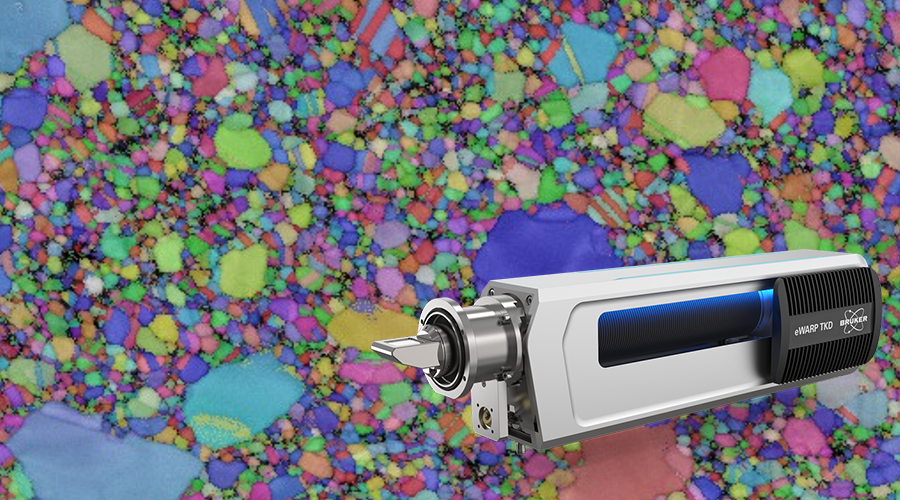
To evaluate the benefits of the recently launched eWARP TKD detector, bismuth (Bi) nanofibers were characterized using on-axis geometry, with both an eWARP TKD detector and a legacy phosphor-screen-based CMOS TKD system (eFLASH OPTIMUS 2).
Conventional off-axis TKD acquisition was not feasible for this material, as the substantially higher beam current required to obtain usable diffraction patterns would rapidly alter the microstructure of the beam-sensitive Bi nanofibers. Owing to its significantly improved signal collection efficiency, eWARP TKD produced indexable diffraction patterns under low-dose acquisition conditions, enabling crystallographic characterization before significant beam-induced structural evolution occurred.
Fig. 1 shows a bismuth nanofiber acquired using eWARP and conventional TKD detectors. Under high electron dose conditions, extensive structural changes were observed. The nanofibers exhibited a significantly higher degree of crystallization, indicating that prolonged electron irradiation had altered the original microstructure. In contrast, low-dose TKD measurements revealed only a limited number of nanoscale crystalline domains embedded within the nanofiber, suggesting that the material remained much closer to its native state.

To further investigate the effect of electron irradiation, fourteen consecutive TKD measurements were performed on exactly the same region using low-dose acquisition conditions. Although each individual scan employed a minimal electron dose, the accumulated dose continuously increased throughout the experiment.
As shown in Fig. 2, the results revealed a clear dose-dependent evolution of the microstructure. With increasing cumulative electron dose, the indexed fraction progressively increased and the apparent crystallinity of the main nanofiber continuously increased.
This experiment highlights a fundamental challenge in the characterization of beam-sensitive materials: the act of measurement can modify the specimen itself. The enhanced sensitivity of the eWARP TKD detector addresses this challenge directly. By producing high-quality diffraction patterns at substantially lower electron dose, the system maximizes the amount of crystallographic information that can be extracted before significant beam-induced transformation occurs. As a result, researchers can characterize beam-sensitive materials with greater confidence that the measured microstructure reflects the original specimen rather than a structure modified by the electron beam.
Sample courtesy of Dr. Ioannis Tzifas from GSI Helmholtz Centre in Darmstadt, Germany


Learn More About eWARP TKD and the eWARP Detector Family
Discover how the eWARP TKD and the eWARP detector family redefine microanalytical performance under challenging, real-world conditions, combining unmatched acquisition speed with high-fidelity signal quality.