Ellipsometry & Reflectometry

Knowledge Pack: Thin Film Characterization with Ellipsometry and Reflectometry

Scroll down to see your full knowledge pack. Save or bookmark this page to re-access your resource collection.
Webinar: Thin Film Characterization Using Spectroscopic Reflectometry and Ellipsometry Techniques

Thin Film Characterization Using Spectroscopic Reflectometry and Ellipsometry Techniques

RESOURCE TYPE: Webinar presentation
LENGTH:
~45 minutes

PRESENTATION HIGHLIGHTS:

  • [00:00:00] Introduction
  • [00:07:20] Ellipsometer and reflectometer technology overview
  • [00:21:23] Applications and case studies
  • [00:31:36] FilmTek product line
  • [00:33:35] Audience Q&A

DESCRIPTION:

Bruker experts discuss and demostrate spectroscopic reflectometry and ellipsometry techniques and the advantages of polarized light methods for measuring thin films — specifically films on silicon and today's complex semiconductor devices (multi-layer/multi-stack). Topics include theoretical fundamentals, accuracy and measurement ranges, Bruker's unique algorithms and hardware implementations, and real-life use cases in both medical device and semiconductor applications.

VIEWERS WILL LEARN:

- How reflectometry and ellipsometry each measure film thickness and material optical properties
- How to get more complete thin-film measurements by combining spectroscopic reflectometry and ellipsometry
- When advanced multi-angle optical techniques are necessary
- Real-world application examples in medical device and semiconductor manufacturing
- Key considerations for instrument selection, including detection limits, metal films, transparent polymers, and turnkey options

Presented by: Chris Claypool, Sr. Director, R&D, FilmTek Products (November 17, 2022)

Application Note: Measuring Thickness of Biologically Active Films for Medical Devices and Sensors

Measuring Thickness of Biologically Active Films for Medical Devices and Sensors

RESOURCE TYPE: Application Note [PDF]
LENGTH:
4 pages

DESCRIPTION:
This application note illustrates how advanced reflectometry and ellipsometry are used to measure film thickness in biomedical device manufacturing. Case studies on glucose sensors, tissue sealers, and blood sensors demonstrate how non-contact, small-spot measurement enables accurate thickness control to the sub-angstrom level across entire production wafers.

READERS WILL LEARN:

  • Why film thickness measurement is critical for medical device manufacturing and patient safety

  • How multi-angle reflectometry and ellipsometry address biomedical film characterization challenges across glucose, tissue, and blood sensor applications

  • Advantages of small-spot, collimated-beam technology for thick coatings and rough substrates

  • How integrated automation (wafer handling, barcode scanning, SECS/GEM software) supports high-volume manufacturing consistency
Webinar: High-Resolution Measurement of Film Thickness and Refractive Index for Silicon Photonics and Planar Waveguide Applications

High-Resolution Measurement of Film Thickness and Refractive Index for Silicon Photonics and Planar Waveguide Applications

RESOURCE TYPE: Webinar presentation
LENGTH:
~1 hour

PRESENTATION HIGHLIGHTS:
  • [00:00:00] Introduction to Silicon Photonics
  • [00:02:38] Introduction to Reflectometry
  • [00:09:42] Introduction to Ellipsometry
  • [00:13:38] Introduction to FilmTek Technology and products
  • [00:22:09] FilmTek Solutions for Silicon Photonics
  • [00:47:01] Conclusion

DESCRIPTION:

Bruker experts introduce advanced multi-angle spectroscopic reflectometry and ellipsometry for the high-resolution thickness and refractive index demands of silicon photonics and planar waveguide applications. The discussion highlights how non-contact FilmTek techniques achieve significantly higher refractive index resolution than conventional prism coupler methods across materials including SiON, Si₃N₄, Ge‑SiO₂, P‑SiO₂, BPSG, APOX, and HiPOX.

VIEWERS WILL LEARN:

- Why precise film thickness and refractive index measurement is critical for photonic device performance
- Advantages and limitations of different measurement approaches for multi-layer photonic structures
- When conventional optical tools reach their limits and how combining reflectometry and ellipsometry at multiple angles overcomes those limitations
- How multi-angle spectroscopic techniques achieve a 10× refractive index resolution advantage over prism coupler methods
- How non-contact methods support R&D characterization and automated in-line process control

Presented by Lawrence Rooney, Senior Application Scientist, Bruker (December 6, 2023)

Video: Optical Metrology for Front-End Semi Process Control

Optical Metrology for Front-End Semi Process Control

RESOURCE TYPE: Video
LENGTH:
~15 minutes

PRESENTATION HIGHLIGHTS:
  • [00:00:10] Introduction to spectroscopic ellipsometry and reflectometry
  • [00:02:30] FilmTek 2000 PAR-SE - Technology for thin-film and multi-layer inspection on silicon and specialty devices
    •   [00:06:53] Thin films and multilayers on patterned device wafers
  • [00:07:14] FilmTek 2000M TSVTechnology for thick film measurement for:
    •   [00:09:45] High aspect ratio TSV structures
    •   [00:11:10] Trench depth
    •   [00:11:42] Film thickness
  • [00:12:17] Unique advantages of Bruker's FilmTek technology
     

DESCRIPTION:

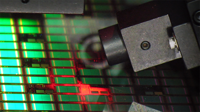
Bruker experts show how FilmTek optical metrology tools — using spectroscopic reflectometry, spectroscopic ellipsometry, and multiple-angle reflectometry — support thin-film characterization for front-end semiconductor process control. The presentation shows how combining multi-angle deep-UV reflectance and ellipsometry data expands measurement capabilities beyond the known limits of individual techniques, with real-world examples from sub-nanometer dielectric films to 200 µm-deep MEMS trench structures.

VIEWERS WILL LEARN:

- How combining reflectometry and ellipsometry removes ambiguity that single techniques cannot
- How to measure ultra‑thin films while resolving both thickness and refractive index
- How non-contact methods support R&D characterization and automated in-line process control
- What to consider when measuring complex multi‑layer stacks such as ONO structures
- How small, collimated measurement spots enable accurate results on patterned wafers
- Advantages and limitations of different measurement approaches for multi-layer photonic structures

Presented by Christopher Claypool, Senior R&D Director, for filmtek Products, Bruker (March 15, 2023)


See all presentations from our Thin Films & Coatings Symposium

Learn More

Find Out More About Our Ellipsometry/Reflectometry Technology