High-Throughput Nanoindentation for Statistical and Spatial Property Determination
Abstract
Standard nanoindentation tests are “high throughput” compared to nearly all other mechanical tests, such as tension or compression. However, the typical rates of tens of tests per hour can be significantly improved. These higher testing rates enable otherwise impractical studies requiring several thousands of indents, such as high-resolution property mapping and detailed statistical studies.
However, care must be taken to avoid systematic errors in the measurement, including choosing of the indentation depth/spacing to avoid overlap of plastic zones, pileup, and influence of neighboring microstructural features in the material being tested. Furthermore, since fast loading rates are required, the strain rate sensitivity must also be considered. A review of these effects is given, with the emphasis placed on making complimentary standard nanoindentation measurements to address these issues.
Experimental applications of the technique, including mapping of welds, microstructures, and composites with varying length scales, along with studying the effect of surface roughness on nominally homogeneous specimens, will be presented.
Authors:
Eric D. Hintsala1, Ude Hangen2, Douglas D. Stauffer1,3
1. Bruker Nano Surfaces, Eden Prairie, MN, USA.
2. Bruker Nano Surfaces, Aachen, Germany.
3. e-mail: douglas.stauffer@bruker.com
JOM 70, 494–503(2018)
doi.org/10.1007/s11837-018-2752-0
© 2018 The Author(s). This article is an open access publication
Introduction
Nanoindentation has been proven to be a powerful tool for exploring mechanical behavior at small-length scales. This is due to the technique being highly localized and only semi-destructive, while simultaneously allowing extraction of a diverse set of properties including elastic, plastic, and fracture. In addition, the sample preparation requirements are significantly less stringent than most other mechanical testing techniques, and the procedures are well established.1–5
However, standard nanoindentation testing requires several minutes per test for tasks such as locating suitable areas, the sample approach, drift correction, and retraction of the tip. This makes certain applications, such as property mapping by indentation grids6,7 or generation of statistical data sets, extremely time consuming and, in some cases, too slow to be practical. Various technologies have been developed in recent years that have greatly accelerated nanoindentation testing, with state-of-the-art speeds of up to 6 indents/ second representing at least two orders of magnitude improvement over standard quasi-static testing. This means that 10,000 indent maps can be completed in less than an hour—for perspective, this would generate a property map of 100 x 100 µm with 1-µm spacing. The speeds, resolution, scan size, and sample preparation requirements are comparable to a variety of SEM mapping techniques, such as electron backscatter diffraction (EBSD) and energy dispersive spectrometry (EDS). The fact that they also give highly complementary information means that correlated surveying of microstructural features for their crystallographic, chemical and mechanical properties provides researchers with a powerful tool. Besides this, statistical indentation techniques allow users to quickly determine parameters of significance, screen materials, and identify more global trends from highly localized nanoindentation tests.8
In addition, statistical data sets help combat factors producing data outliers, such as surface roughness,9–12 which are a hindrance to accurate nanoindentation testing. Lastly, these techniques can also be applied to systems with environmental control, such as heating, controlled humidity, or even submerged specimens, providing additional variables to explore. To date, hardness mapping has been utilized to explore spatial variations in a variety of materials including cement pastes,13 concrete,14 tooth enamel,15 metal matrix composites,6,7,15,16 intermetallics,17 metal alloys,6,18,19 and wood adhesive bonds.20 However, properly conducting high-speed nanoindentation and interpreting its results requires one to consider various factors, such as indentation spacing, strain rate effects, and indentation depth.
In addition, it can currently only be applied to measuring hardness and elastic modulus because of the restrictions on load function choice. Thus, high-speed indentation is not a replacement for standard indentation techniques. Rather, the approach that is advocated is that of a complementary technique for standard indentation, where the standard testing protocol allows one to assess indentation size effects,21–23 rate dependence,24 and spacing effects. Here, we will review these key concepts first before presenting example application data emphasizing property-mapping techniques.
Experimental Considerations for Nanoindentation Mapping
To produce high-quality property maps, consideration of the stress field underneath the indenter tip is critical. Not only is there potential for the damage zones from individual tests to overlap and invalidate the results, but the ‘‘resolution’’ of the nanoindentation test is relevant when testing near boundaries of features, such as grain and phase boundaries, weld zones, composite interfaces, and material gradients, for damage or composition.
The indenter resolution needs to be carefully defined, as the stress field occurs in three dimensions and consists of separately sized elastic and plastic zones. A second consideration involves the necessity of high loading rates, which may induce strain rate sensitivity changes in the measured hardness. Both subjects will be covered in the following two sections, ‘‘Indentation Spacing and Resolution’’ and ‘‘Strain Rate Sensitivity’’.
Indentation Spacing and Resolution
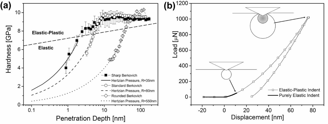
When mapping surface properties, the in-plane spatial resolution is of primary concern; however, defining this requires consideration of the full three-dimensional shape of the indentation stress field or the volume of material being tested. Since the stress field decays continuously as a function of distance from the contact zone, boundaries can only be defined by a specific stress or strain value. The most important is the subdivision into a purely elastic25 and an elastic–plastic zone with the boundary set by the yield criterion of the material,26 as illustrated in Fig. 1. Thus, the entire elastic zone contributes to the modulus measurement, while only the elastic–plastic zone contributes to the hardness, H, measurement. In terms of a more practical definition for defining the indentation resolution, one can define an acceptable relative change of properties in proximity to a feature, such as a microstructural boundary or a previous indent.
Some indenters have a geometry that can be described as self-similar, which is simply a tip shape with a constant ratio of the contact area to depth versus load. This property is maintained by common pyramidal indenters, including Berkovich and cube corners, as well as conical tips, and implies that the measured properties will not change as a function of indentation load. Notably, spherical tips are an exception. Thus, for a self-similar indenter, all-important geometrical parameters can be expressed as a function of the contact radius, a. The contact radius is defined as the radius of a circle of estimated equivalent area to that of the actual contact, thus allowing pyramidal probes to be described by the same parameter as spherical and conical.
Regarding issues with indent-to-indent spacing, there are several effects. If the second indent overlaps with the residual impression or pileup from the previous, this clearly invalidates the semi-infinite half-space assumption and the actual contact radius will deviate significantly from the assumed value. Subtler is the overlap of plastic zones, which extend further in the sub-surface of the testing plane. The residual plastic zone could be considered cold-worked, thereby elevated hardness, but the exact interaction of plastically nucleated defects could also produce a softening effect by providing dislocation sources. The radius of the plastic zone, Rp, in relationship to the contact radius is material specific because of differences in plasticity mechanisms. For metals, this ratio can range from 3a to 6a.27–29 For a sharp Berkovich tip with 50-nm radius of curvature, reliable hardness measurements can be achieved at a depth of at least 15 nm as shown in Fig. 1 (note that the modulus was constant for the three tips over the entire depth range). This corresponds to a maximum contact radius of 57 nm, thus requiring a 315-nm indent spacing for a soft metal with Rp ~ 6a. This situation improves for a cube corner that has a steeper contact radius to a depth ratio of 0.7 compared to 3.5 for a Berkovich. Since these tips are self-similar, the plastic zone size is proportional to the contact radius and is reduced by approximately a factor of 5 as well. As previously discussed, the exact plastic zone size is specific to a given tip-material-depth combination, so experimental evaluation is required to determine this size precisely. This can be illustrated by two case studies: (1) the influence of one indentation on its neighbor and (2) the influence of interfaces in the proximity of an indent.
To illustrate this effect, the indent spacing, d, was varied on an Al sample as tested with a Berkovich tip, as shown in Fig. 2a. Interestingly, reducing d results in a corresponding decrease in hardness rather than an increase as would be expected for work hardening. Additionally, no effect on modulus would be expected from plastic zone overlap. Therefore, the effect on modulus at the smaller values of d indicates the invalidation of the area function due to pileup. This pileup-affected zone begins at d = 750 nm, slightly less than the recommended distance of 5.6 times the contact radius, or 840 nm for a maximum displacement of 50 nm. Clearly, a trade-off occurs between lateral resolution and hardness measurement accuracy, as using a sharper tip at smaller depths gives a reduced elastic–plastic zone. An additional trade-off can be made by sacrificing the hardness measurement altogether and limiting testing to a purely elastic regime. The absence of a plastic zone and residual displacement and thus no pileup in a purely elastic indent allow for the contact radii to overlap between individual indents.
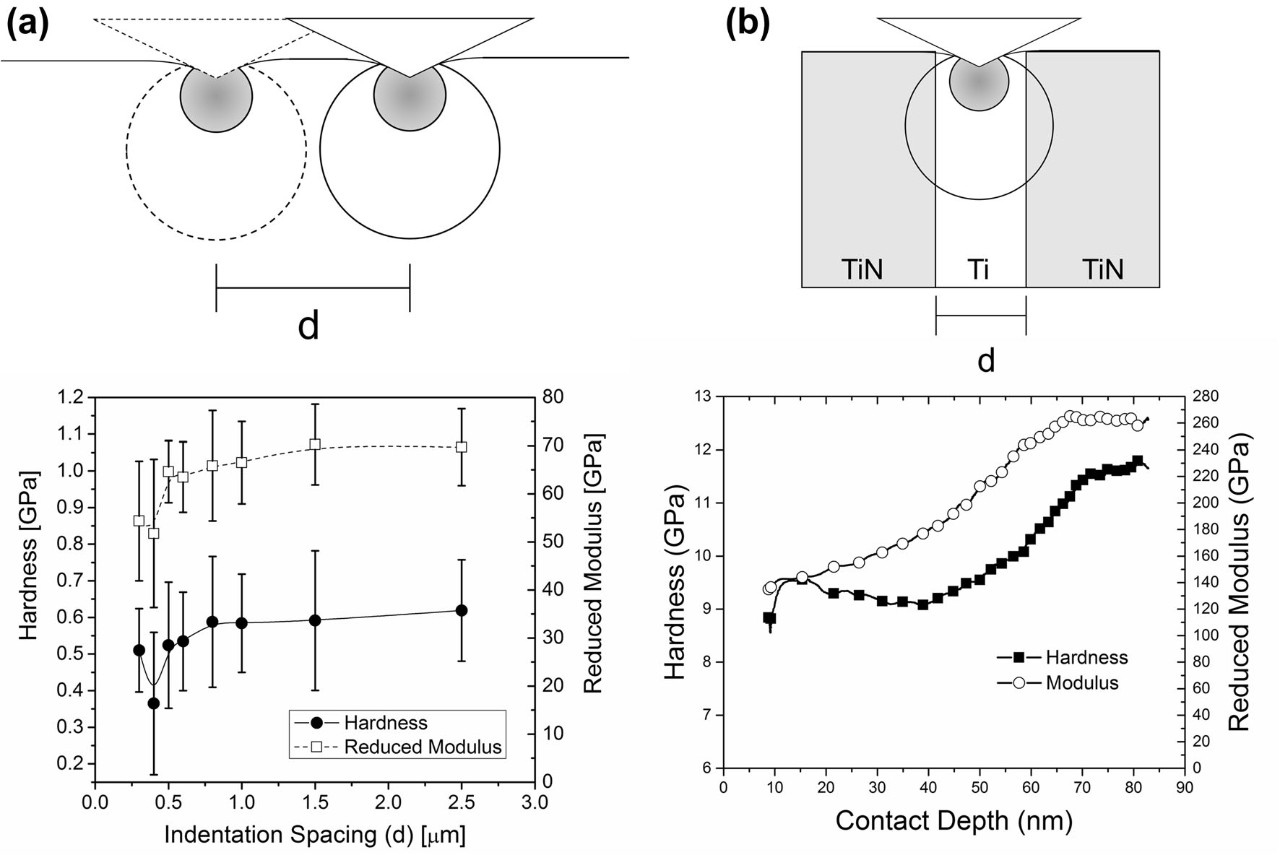
The role of sample interfaces, important to high-resolution mapping of compositional and phase varied materials, is illustrated by mapping with a metal-ceramic cross-sectional sample. Here, indents are placed near a material interface in a sample, specifically, a 750-nm-wide Ti layer sandwiched between two extremely hard (H ~ 25 GPa) Ti-N layers. The indenter was carefully placed in the center of the Ti layer using in situ SPM imaging. A profile of hardness and modulus as a function of depth is shown in Fig. 2b, where correct hardness and reduced modulus values for Ti were only measured at 15–30-nm depth. At larger depths, the indentation stress field increasingly interacts with the TiN layers resulting in increasing modulus and hardness values. In some mapping scenarios, the indentation grid is generated with a predetermined spacing that will place indents at varying distances from, or on top of, a phase boundary or interface in the sample. This can produce measurement errors if plasticity mechanisms are affected by the presence of the boundary, such as providing defect sources, sinks, and barriers. These data points can usually be filtered during analysis by examining the statistical distribution of measured properties and removing outliers. These boundary effects can change the ideal indent spacing for mapping. Therefore, examining the effect near sample boundaries to determine the best spacing value is recommended.
To summarize this section, the achievable limits of nanoindentation resolution depend strongly on the tip shape, material being tested, and, crucially, the deformation regime. Following Jakes et al.,30,31 three dimensionless parameters can be defined that control indent resolution: the contact area relative to the distance to a feature, √A/d, and two material-dependent parameters, the ratio E/H and the Poisson’s ratio. One can define a maximum modulus or hardness change versus d using these parameters. Therefore, the smallest achievable d values are found at the lowest indentation depths in the elastic regime. However, if hardness measurements are desired, testing in the elastic–plastic regime is necessary and a balance between the accuracy of hardness and lateral resolution must be chosen.
Strain Rate Sensitivity
One of the drawbacks of high-speed nanoindentation mapping is a loss of flexibility in the load function, where high loading rates are needed for increased mapping speed. These high loading rates can influence the measured hardness, but this depends again on the material type, tip shape, and several other variables. The hardness from a nanoindentation test is strain rate dependent and fit by a power law relationship by a characterizing parameter, m ~ ∂lnH/∂lnε̇ , where ε̇ is the strain rate. The strain rate for indentation is defined proportionally as the displacement rate over the total displacement ḣ/h or ½Ṗ=P24 correspondingly for loading rate over total load for materials that do not have depth dependence to their response, and for self-similar indenters. Since this relationship is fit by a power law, one can describe it as an order of magnitude effect.
As previously discussed, high-speed nanoindentation techniques can run about two orders of magnitude faster than standard indentation techniques. Since typical strain rate sensitivity parameter m values range from 0.001 to 0.1 in crystalline materials, this corresponds to a hardness value shift between 0.4% and 37% compared to standard speed indentation. However, one must look at the bigger picture, which is that strain rate sensitivity is determined by the predominant deformation mechanism and is strongly affected by variables that aid or hinder operation of these mechanisms. These variables most notably include temperature, but also crystalline orientation and grain size. Special cases, such as nanocrystalline or ultrafine grain materials, can possess high strain rate sensitivity values32 because of the dominance of grain boundary diffusion mechanisms or, in the case of glasses, unusual behavior due to shear transformation zones.33,34 Some literature data are presented in Table I, which shows how much of a hardness shift would be expected by increasing the strain rate by two orders of magnitude as discussed above for some of the more interesting scenarios.
Thus, the origins of strain rate sensitivity are complex and require considerations of many subtleties. However, for several classes of materials the effect is essentially marginal. The best approach is to directly measure the strain rate sensitivity for the materials of interest; these techniques have recently been reviewed by Maier-Kiener and Durst.39 As a final point, the role of indentation depth should be acknowledged, as shallower indents are typical for indentation mapping and deeper indents for strain rate sensitivity measurements. Ideally, this should not affect results but as real tips are blunt, shallower indents are increasingly dominated by a spherical-like contact.
Hardness change expected for two orders of magnitude increase in loading rate.
| Material | m | ΔH (%) | Notes | References |
| UFG Al | 0.03 to 0.1 | 14 - 37 | From RT - 250°C | 32 |
| Single crystal Cr | 0.08 to 0.003 | 37 - 1.4 | From RT - 300°C | 35 |
| Ti alloy | 0.005 to 0.04 | 2 - 18 | Different grain orientations | 36 |
| Al-Li alloy | -0.01 to 0.0035 | 4.6 - 1.6 | Different aging recipes | 37 |
| Fused silica | 0.0068 to 0.01 | 3.1 - 4.6 | Room temperature | 38 |
Summary and Complimentary Nanoindentation Validation
In the absence of sophisticated analysis and/or modeling, one can simply advocate the approach of exploring the effects of the parameter space on the measured properties of interest whenever possible, specifically, the combination of loading rate, indentation depth, and indentation spacing. Thus, a typical complimentary approach to validate a high-speed indentation map would include:
- Measurement of depth sensitivity: Depth profiling is already frequently done to calibrate tip area functions. A variety of methods can be used, including a varying depth indent arrays, partial unload load functions, or dynamic methods.40,41
- Measurement of spacing sensitivity: With the depth dependence established, the user can chose their desired depth for the indentation map. Next, the spacing effects at that desired depth can be studied with indent arrays. When high spatial resolution is unnecessary or impractical because of the desire to map a larger area by nanoindentation, conservatively large spacing could be used freely.
- Measurement of rate sensitivity: Either through grids with varying indent speed or characterizing the strain rate sensitivity coefficient.39
There could also be a desire to define the desired indent spacing first, i.e., resolution of the map, then what maximum depth can be used needs to be determined, thereby reversing steps 1 and 2.
Applications for Nanoindentation Mapping
In the following, several examples are presented that highlight the capabilities of state-of-the-art high-speed nanoindentation. The following examples were all performed using a Hysitron TI 980 TriboIndenter (Bruker Nano Surfaces, Minneapolis, MN, USA) operating in Accelerating Property Mapping (XPM) mode.
Correlated EBSD and Nanoindentation Mapping
The most obvious application for such technology is mapping of small-scale material interfaces as they cannot be easily evaluated at the bulk scale. These include welds, especially microscale ones as produced by laser and resistance techniques, mapping of phases, and grains in alloys, and evaluation of composites. In particular, dissimilar material welds produce complex microstructures42 and can be better engineered using nanoindentation data to establish statistically significant variables.43
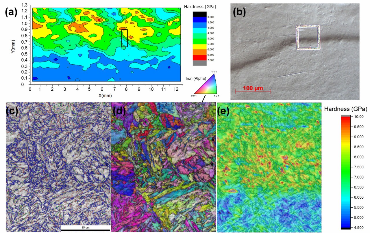
The scale and resolution of high-speed indentation can be demonstrated through a correlated EBSD and nanoindentation map of a 410 stainless steel, which was laser clad onto a 4140 stainless steel substrate. The large-scale structure of the heat-affected zone from the laser cladding process is shown via a traditional stage automation method in Fig. 3a. To investigate the transition from the cladding to the substrate in more detail, a fiduciary marker was drawn around the interface using focused ion beam machining to facilitate testing of the same region by nanoindentation mapping and EBSD. In this case, a Berkovich tip was used with 400 µN force and an indent spacing of 500 nm. The nanoindentation mapping shows little difference in modulus between the cladding and the substrate, but a substantial change in hardness with ~ 5 GPa average for the 4140 substrate and ~ 8 GPa hardness average for the cladding. In the correlated EBSD boundary map, it appears that the region of highest hardness corresponds closely with regions of a high density of high-angle grain boundaries, marked in blue.
High-Speed Nanoindentation at Elevated and Cryogenic Temperatures
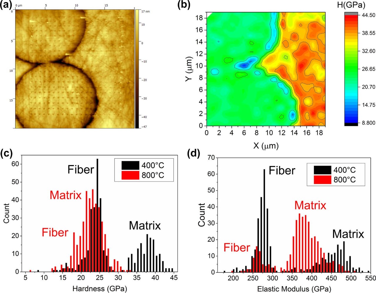
High-temperature nanoindentation is a growing field of research for reactors, engines, turbines, and more. One popular high-temperature material, a SiC matrix and SiC fiber composite, is evaluated at high temperature using 5-µm indent spacing, 7-mN load, and a Berkovich tip. The difference in hardness between the fibers and the matrix is apparent, along with a region of low hardness along the interface (Fig. 4). This is likely due to free volume along the fiber/matrix interface, reducing the hardness through decreased material confinement. The distributions of hardness and modulus at 400°C show a bimodal distribution, individually corresponding to the fiber and matrix. As the temperature is increased to 800°C, the modulus values shift slightly downward overall, as expected, but maintains a bimodal distribution. The two measurements were taken from different regions of the sample, so the change in total counts for the two phases is different. More interestingly, the hardness distribution is observed to shift towards a single peaked distribution at 800°C.
Cryogenic temperatures are of interest for materials that are subjected to conditions such as outer space, arctic or winter environments, and part of cooling systems. A ubiquitous structural alloy, 1018 steel, was studied from room temperature down to -120°C. A hardness map at 0°C generated with 1-µm indent spacing, a peak load of 500 µN, and a Berkovich tip clearly shows the two-phase ferrite and pearlite microstructure, which is also reflected by the hardness distribution as seen in Fig. 5. Indents into the ferrite phase were done as part of a decreasing temperature sweep, with the resulting load displacement curves indicating a ductile-to-brittle transition at -58°C. Here, homogeneous dislocation plasticity at the above temperatures gave way to serrated flow, indicating dislocation bursts. Since ferrite is BCC, the Peierls’ barrier is relatively large compared to FCC metals and is thus reliant on thermal assistance for homogeneous plasticity.
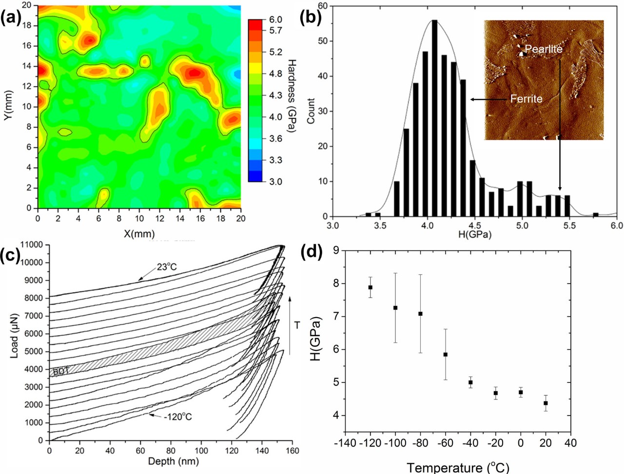
This was also reflected in the hardness, which increased 44% over the tested temperature range. This hardening for decreasing temperatures also relates to the ductile to brittle temperature transition. This transition is more obvious when looking at the pop-in behavior of the indentation curves.44 The room temperature behavior is primarily a smooth curve or with very short pop-ins to approximate a predominately smooth curve. As temperatures decrease, the flow becomes more stochastic with increasing pop-in size. There seems to be a transition between the -15°C and -25°C curves. This DBTT is lower than the 5°C value typically reported for Charpy impact testing, which is a much higher strain rate.
High-speed nanoindentation techniques provide an advantage when operating at extreme non-ambient temperatures through reduced contact time, which reduces tip wear, and the relative effect of drift. Tip-sample thermal equilibrium is one of the largest challenges to extreme temperature testing as it produces drift when they are brought into contact. The cryo and high-temperature stage in this article utilizes a multi-element heating microchamber45 that exposes the tip and sample to the same environment. However, it has been shown46,47 that thermal stabilization in vacuum is more time consuming and difficult. Reducing the typical time in contact from 20 s to 0.2 s reduces the effect of drift on the measurement by two orders of magnitude. This reduced time in contact also significantly reduces tip wear, a major issue of high temperature testing.48 The tip sample contact can be modeled as a high-pressure diffusion couple in thermodynamic software such as Thermal Calc. Simply reducing the time in contact has a dramatic impact on the number of indentations that can be performed with a given tip/sample combination.
Generation and Utilization of Large Data Sets
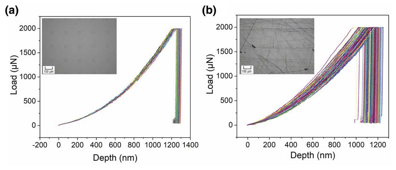
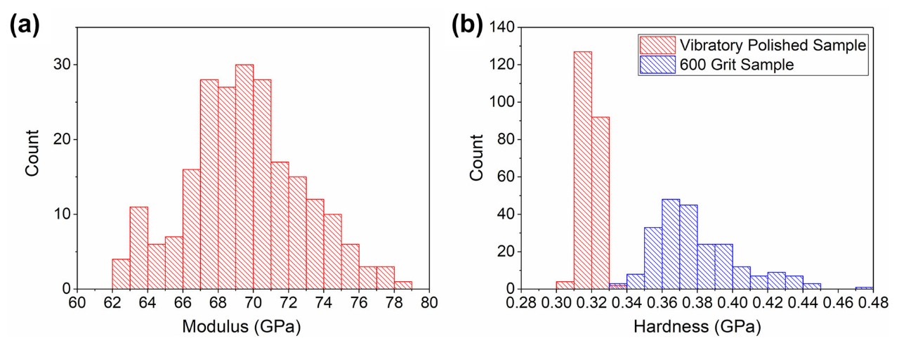
In contrast to the heterogeneous samples tested thus far, nanoindentation is often performed on samples that are relatively homogeneous, such as foils, thin films on substrates, and the substrates themselves. Even a layered sample with large dimensions in the sample plane can be considered locally homogeneous. In these cases, statistics allow for generation of large data sets where the precise values can be determined, with data histograms allowing for the identification of statistical outliers. This can be compared to the number of tests run in a typical nanoindentation study, where n ≤ 10 in many cases. A simple experiment can be done looking at the statistical distribution of hardness and modulus comparing vibratory polished (100) aluminum and aluminum polished with 600 grit paper. Arrays of nine indents, 3 x 3 with 15-µm spacing between indents, are placed in a larger 5 x 5 array (Fig. 6).
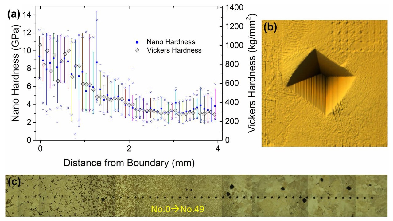
The total number of indents is now n = 225 for each sample, which is a factor of a 20 times larger number of tests than for most nanoindention studies. The pileup corrected modulus and hardness histograms (Fig. 7) show both an increase in hardness for the roughened/work-hardened sample and a corresponding increase in the spread of the data. Combining both statistical analysis and mapping compared against high-speed nanoindentation for a railway weld joint in a railway steel can be compared to traditional Vickers microhardness testing.49–51 Here, 196 indent grids produced by high-speed nanoindentation with 5-mN load and a Berkovich indenter are compared against a single Vickers indent in a line scan starting in the weld joint and moving progressively through the heat-affected zone, using an empirical relationship to compare hardness.52 The grid of nanoindentations fit into approximately the same area as the single microhardness test (Fig. 8). In this case, a variety of microstructures are encountered, from martensitic rich regions near the weld joint progressively into bainite and finally ferrite. It can be observed that although the hardness versus distance curves are comparable between the average value of the high-speed nanoindentation grids and microindentation, the grids feature scatter bands due to the varying microstructure. For instance, the spread is increased near the weld joint, as the martensite clustered into islands around the grain boundaries, where as bainite and ferrite represent better dispersed microstructures. In these regions, a researcher could consider moving to more of a mapping rather than statistical sampling type of experiment.
Conclusions and Outlook
Overall, high-speed indentation techniques are relatively underused given they possess many potential applications. Property mapping, especially when used in conjunction with correlated techniques characterizing the structure, provide detailed information on small-scale regions of significant industrial importance that are not easily tested on the bulk scale, such as welds, fine grain and phase structures, composites and interfaces, and more. Statistical distributions can be generated simultaneously, which offer a variety of useful information. However, these techniques do not replace standard nanoindentation techniques, as the influence of the indentation size effect from depth, strain rate sensitivity, and spacing should be studied in conjunction.
Looking forward, there are many relatively unexplored applications for these techniques. Though there are a multitude of material microstructures to potentially map and model, it is the authors’ opinion that sophisticated analysis of ‘‘big data’’ sets, through techniques like machine learning, represent one the biggest frontiers in materials science. The theme of bridging length scales and producing cohesive understanding of bulk mechanical behavior based on nanoscale measurements is very attractive and may lead to future breakthroughs in materials design and fine-tuning of their performance. As a rapid and highly localized mechanical measurement tool, high-speed nanoindentation mapping should play an important role in this regard.
Acknowledgements
The authors gratefully acknowledge assistance from Richard Nay, Jared Risan, Robert Dietrich, Anqi Qiu, and Benjamin Stadnick with the specimen testing and Daniel Sorensen with sample preparation.
Open Access
This article is distributed under the terms of the Creative Commons Attribution 4.0 International License, which permits unrestricted use, distribution, and reproduction in any medium, provided you give appropriate credit to the original author(s) and the source, provide a link to the Creative Commons license, and indicate if changes were made.
No changes were made to the original text or images. Layout changes were made to accommodate the web page.
Funding
Funding was provided by Bruker Nano Surfaces.
References
1. W.C. Oliver and G.M. Pharr, J. Mater. Res. 7, 1564–1583 (1992).
2. A.C. Fischer-Cripps, Surf. Coat. Technol. 200, 4153–4165 (2006).
3. A.A. Volinsky, J.B. Vella, and W.W. Gerberich, Thin Solid Films 429, 201–210 (2003).
4. G.M. Pharr, D.S. Harding, and W.C. Oliver, Mechanical Properties and Deformation Behavior of Materials Having Ultra-Fine Microstructures, ed. M. Nastasti, D.M. Parkin, and H. Gleiter (Dordrecht, the Netherlands: Kluwer Academic Publishers, 1993), pp. 449–461.
5. W.C. Oliver and G.M. Pharr, J. Mater. Res. 19, 3–20 (2011).
6. N.X. Randall, M. Vandamme, and F.J. Ulm, J. Mater. Res. 24, 679–690 (2009).
7. G. Constantinides, K.S. Ravi Chandran, F.J. Ulm, and K.J. Van Vliet, Mater. Sci. Eng., A 430, 189–202 (2006).
8. L. Sorelli, G. Constantinides, F.J. Ulm, and F. Toutlemonde, Cem. Concr. Res. 38, 1447–1456 (2008).
9. J.A. Greenwood and J.H. Tripp, Trans. ASME Ser. E J. Appl. Mech. 34, 417–420 (1967).
10. W.G. Jiang, J.J. Su, and X.Q. Feng, Eng. Fract. Mech. 75, 4965–4972 (2008).
11. M.S. Bobji and S.K. Biswas, J. Mater. Res. 14, 2259–2268 (1999).
12. A.C. Fischer-Cripps, Factors Affecting Nanoindentation Test Data (New York, NY: Springer, 2000), pp. 61–82.
13. M. Sebastiani, R. Moscatelli, F. Ridi, P. Baglioni, and F. Carassiti, Mater. Des. 97, 372–380 (2016).
14. J.L. Cuy, A.B. Mann, K.J. Livi, M.F. Teaford, and T.P. Weihs, Arch. Oral Biol. 47, 281–291 (2002).
15. K. Morsi, V.V. Patel, K.S. Moon, and J.E. Garay, J. Mater. Sci. 43, 4050 (2008).
16. H. Engqvist and U. Wiklund, Tribol. Lett. 8, 147–152 (2000).
17. H.-W. Chang, M.-X. Zhang, A. Atrens, and H. Huang, J. Alloys Compd. 587, 527–532 (2014).
18. C. Tromas, M. Arnoux, and X. Milhet, Scripta Mater. 66, 77–80 (2012).
19. T. Ogura, S. Hirosawa, and T. Sato, Sci. Technol. Adv. Mater. 5, 491–496 (2004).
20. J. Konnerth, A. Valla, and W. Gindl, Appl. Phys. A Mater. Sci. Process. 88, 371–375 (2007).
21. W.W. Gerberich, N.I. Tymiak, J.C. Grunlan, M.F. Horstemeyer, and M.I. Baskes, J. Appl. Mech. 69, 433 (2002).
22. W.D. Nix and H. Gao, J. Mech. Phys. Solids 46, 425–441 (1998).
23. M. R. Maughan, A. A. Leonard, D. D. Stauffer, D. F. Bahr, Philos. Mag. (2017). doi.org/10.1080/14786435.2017.1322725.
24. B. N. Lucas, W. C. Oliver, G. M. Pharr, J.-L. Loubet, MRS Online Proc. Libr. 436 (1996).
25. H. Hertz, Hertz’s Miscellaneous Papers (London, UK: Macmillan, 1896).
26. K.L. Johnson, Contact Mechanics (Cambridge, UK: Cambridge University Press, 1985).
27. K. Durst, B. Backes, and M. Göken, Scripta Mater. 52, 1093–1097 (2005).
28. ASTM Standard E384-17, Standard Test Method for Knoop and Vickers Hardness of Materials, (West Conshohocken, PA: ASTM International, 2017) doi.org/10.1520/e0384-17.
29. DIN ISO 6507-1:2018, Metallic materials—Vickers hardness test—Part 1: Test method (Geneva, Switzerland: International Organization for Standardization, 2018).
30. J.E. Jakes, J. Mater. Res. 24, 1016–1031 (2009).
31. J.E. Jakes and D.S. Stone, Philos. Mag. 91, 1387–1399 (2011).
32. J.M. Wheeler, V. Maier, K. Durst, M. Göken, and J. Michler, Mater. Sci. Eng., A 585, 108 (2013).
33. J. Lu, G. Ravichandran, and W.L. Johnson, Acta Mater. 51, 3429–3443 (2003).
34. F.J. Dalla Torre, A. Dubach, M.E. Siegrist, and J.F. Löffler, Appl. Phys. Lett. 89, 091918 (2006).
35. V. Maier, A. Hohenwarter, R. Pippan, and D. Kiener, Scripta Mater. 106, 42 (2015).
36. T.-S. Jun, D.E.J. Armstrong, and T.B. Britton, J. Alloys Compd. 672, 282 (2016).
37. H. Ovri and E.T. Lilleodden, Acta Mater. 89, 88 (2015).
38. R. Limbach, B.P. Rodrigues, L. Wondraczek, and J. Non-Cryst, Solids 404, 124 (2014).
39. V. Maier-Kiener and K. Durst, JOM 69, 2246–2255 (2017).
40. S.A.S. Asif, K.J. Wahl, and R.J. Colton, Rev. Sci. Instrum. 70, 2408 (1999).
41. X. Li and B. Bhushan, Mater. Charact. 48, 11–36 (2002).
42. L.E. Murr, J. Mater. Eng. Perform. 19, 1071–1089 (2010).
43. B. Jones and C. Nachtsheim, J. Qual. Technol. 43, 1–15 (2011).
44. O.L. Warren, S.A. Downs, and T.J. Wyrobek, Z. Metallkd. 95, 287–296 (2004).
45. U.S. Patent, US 20150185117 A1, Environmental conditioning assembly for use in mechanical testing at micron or nano-scales, Jul 2, 2015.
46. J.M.Wheeler, D.E.J.Armstrong, W.Heinz, and R.Schwaiger, Curr. Opin. Solid State Mater. Sci. 19, 354–366 (2015).
47. S. Korte, R.J. Stearn, J.M. Wheeler, and W.J. Clegg, J. Mater. Res. 27, 167–176 (2012).
48. J.M. Wheeler and J. Michler, Rev. Sci. Instrum. 84, 101301 (2013).
49. R.R. Ambriz, D. Chicot, N. Benseddiq, G. Mesmacque, and S.D. De la Torre, Eur. J. Mech. A Solids 30, 307–315 (2011).
50. K.H. Chung, W. Lee, J.H. Kim, C. Kim, S.H. Park, D. Kwon, and K. Chung, Int. J. Solids Struct. 46, 344–363 (2009).
51. G. Sun, F. Xu, G. Li, X. Huang, and Q. Li, Comput. Mater. Sci. 85, 347–362 (2014).
52. DIN ISO 14577-1:2015, Metallic materials—Instrumented Indentation Test for Hardness and Materials Parameters—Part 1: Test Method (Geneva, Switzerland: International Organization for Standardization, 2015).