Elemental Analysis of Thin Films & Coatings
Chemical Identification
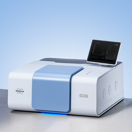
There are numerous methods to chemically identify films and coatings using FTIR spectroscopy. These are transmittance, attenuated total reflection (ATR), gracing angle reflectance (GIR) or infrared reflection absorption spectroscopy (IRRAS), polarization modulated IRRAS (PMIRRAS). Depending on the film thickness, optical property and supporting substrates different measurement mode(s) can be preferentially applied.

Analyze Metallic Coatings

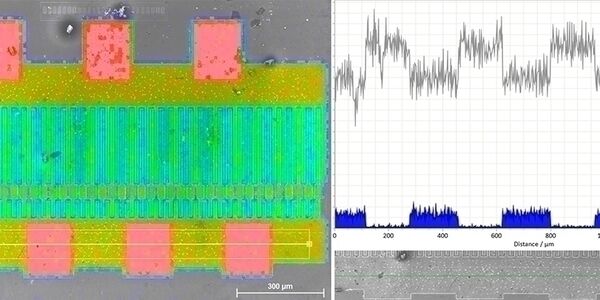
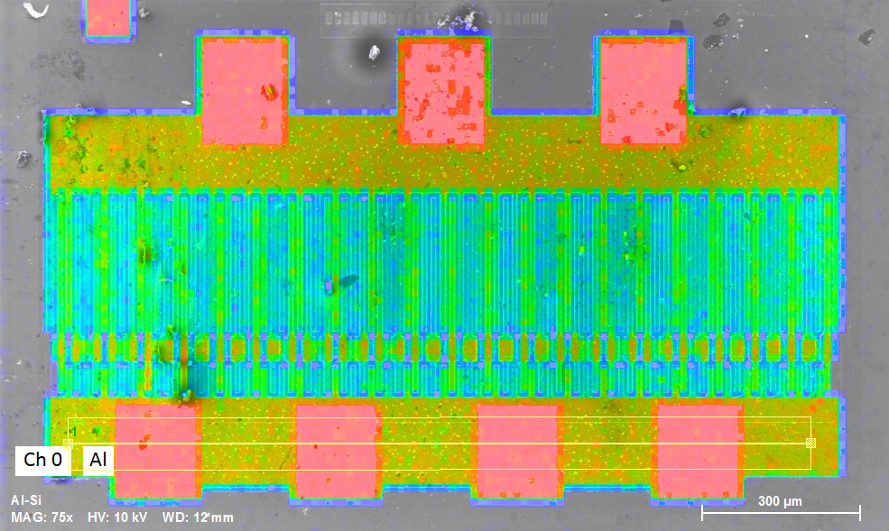
Metallic coatings are used as environmental barriers, actively protecting an underlying material from degradation. In engineering and construction materials they are applied on structural metals and alloys. For optical devices, they are used as mirrors and silvering in headlight reflectors. Metallic coatings are also found in everyday objects such as eyeglasses, utensils, watches, jewelry and toys. The properties of these coatings largely depend on their thickness, crystalline structure, chemical composition and mechanical endurance. Bruker offers a wide range of analytical tools for electron microscopy or as standalone to facilitate the development of such coatings. For example with micro-XRF for quantitative analysis of metallic multilayer stacks for composition and coating thickness.
And electron microscope analyzers (EDS, EBSD, WDS) for fast and reliable quantitative chemical and structural anaysis.
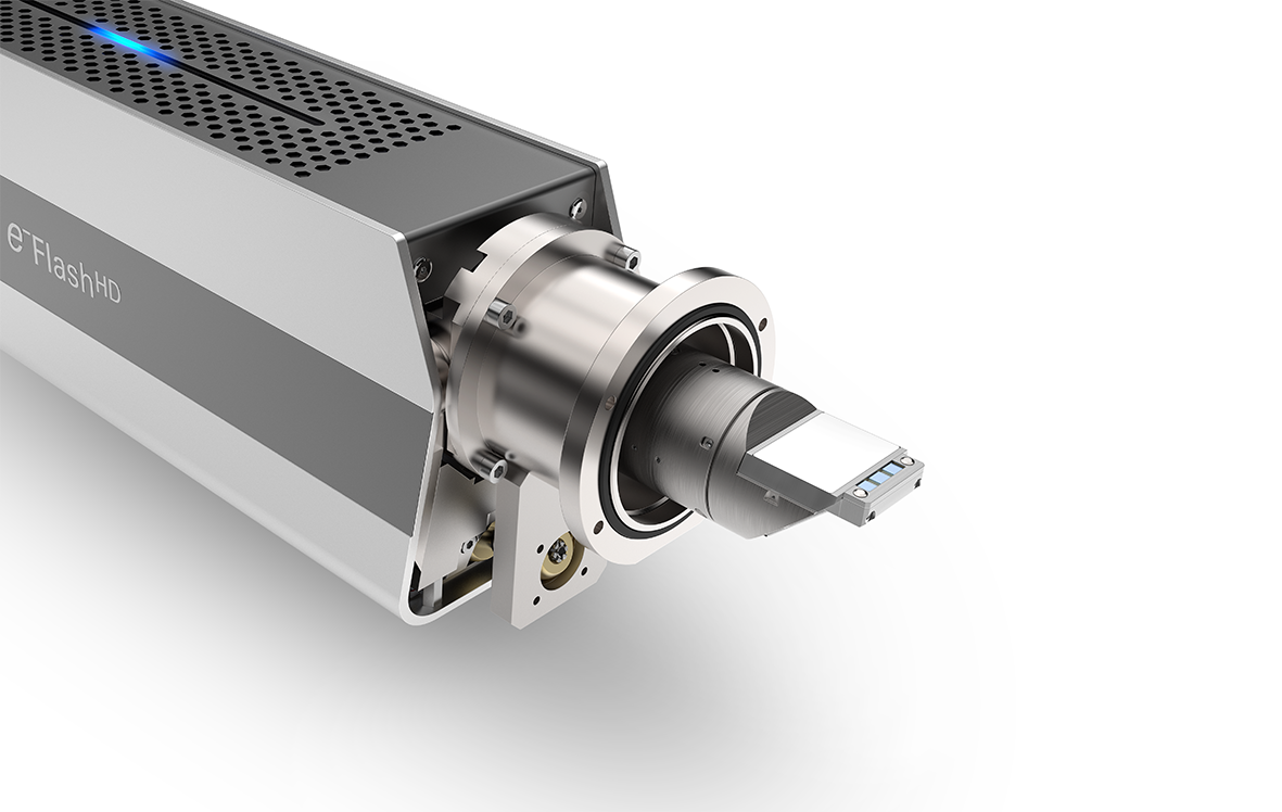
Quantitative Characterization of Nanostructured Thin Films with On-axis TKD
Nanomaterials are usually investigated in the Transmission Electron Microscope (TEM). However, it is possible to characterize nanomaterials quantitatively by benifiting from the large field of view of the Scanning Electron Microscope (SEM). The on-axis TKD technique was developed to this aim; it is now a well established SEM-based method producing orientation distribution measurement at the nanoscale using EBSD hardware. In this application example, the orientation distribution of gold and platinum thin films were measured with
e-Flash FS detector retroffited with OPTIMUS TKD head in a FEG-SEM. High speed TKD measurement are achieved at low probe current (<3 nA) allowing to overcome beam drift and achieve ultra high spatial resolution: in 20 minutes over 1000 grains were measured with the smallest grain size being 20 nm and ultrafine features such as twin boundaries were resolved (3nm).