
Layer Thickness Analysis of Thin Metal Coatings with micro-XRF on SEM
Layer Thickness Analysis of Thin Metal Coatings
Micro-XRF is a common used non-destructive analytical method for measuring the film thickness of different kinds of samples without any sample preparation. Additionally, the composition of the layer can be determined at the same time. Examples of such applications are: connector pins or solder bumps on PCB boards, lead frames and chip carriers, coatings on solar cells or even coatings that are used as corrosion protection for different kinds of materials. Both, the non-destructive operation of the method and the ability of X-rays to penetrate into the sample and obtain information on the material beneath the surface make this method attractive for the thickness and composition analysis of single and multiple layers.
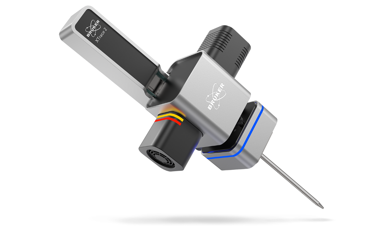
This webinar will discuss the development of layer models in the XMethod software module and the application of such analytical methods using the XTrace, a micro-XRF source attachment to an SEM. The focus will be on showing several application examples, such as metallic coatings on different substrates, Au/Ni coating on copper on a printed circuit board (PCB). Compound layers of solar cells will also be discussed. A comparison of results for calibration standards will be performed in order to demonstrate precision and reproducibility.
This webinar will be round off by a 15-minute Q&A session where our experts will answer your questions.
Who Should Attend?
Speakers
Dr. Max Buegler
Application Scientist Micro-XRF, Bruker Nano Analytics
Stephan Boehm
Product Manager - micro-XRF on SEM and WDS, Bruker Electron Microscope Analyzers
Watch this Webinar On-Demand
Please enter your details below to gain on-demand access to this webinar.
