Multiple Leading Logic and Foundry Customers Order Bruker X-Ray Defect Inspection Systems
Crystalline Defect Detection and Classification Capabilities of JVSensus-600E Enable Yield Improvement of Advanced Technology Nodes
SAN FRANCISCO, California – July 11, 2017 – At SEMICON West 2017, Bruker’s Semiconductor Division today announced that leading multiple semiconductor manufacturers have ordered JVSensus-600E X-ray Diffraction Imaging Systems for in-line wafer monitoring of crystalline defects. The JVSensus-600E tool is equipped with both high-speed and high-resolution X-ray diffraction imaging (XRDI) measurement capabilities for detecting and classifying a wide range of crystalline defects induced by high-stress processes, such as fast annealing and CMP, or by poor wafer handling. The JVSensus system allows defects to be identified prior to annealing, which is often the critical step that leads to wafer breakage and severe yield loss. By detecting defects early in the process, semiconductor manufacturers can quickly identify the root cause of processes causing wafer breakage and reduce yield loss.
“We are delighted to have been selected by industry-leading customers to provide defect inspection systems for their production yield improvement,” said David V. Rossi, President of the Bruker Semiconductor Division. “We see these shipments as further validation of the value that early detection of critical defects brings to our customers in reduction of wafer breakage."
“As the industry utilizes more aggressive steps within more advanced technology nodes, such as fast annealing strategies, new non-visual defect detection challenges arise,” added Isaac Mazor, Vice President and General Manager of Bruker’s X-ray Semiconductor business. “The JVSensus-600E system is capable of detecting a wide range of crystalline defects using X-ray diffraction imaging technique, and is optimised for both blanket and pattern wafers on a single system. This allows a fab to efficiently ramp up processes and quickly identify crystalline defects on product wafers to minimize yield loss from wafer breakage in their production line."
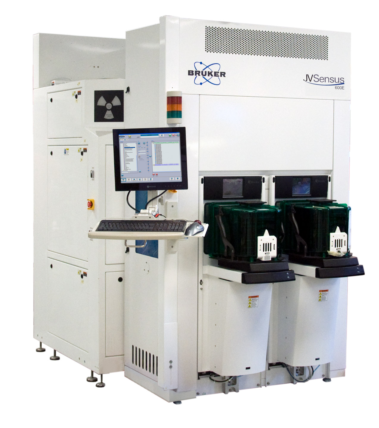
About JVSensus-600E
JVSensus-600E is a production-worthy XRDI system for detecting and classifying crystalline defects in single crystal wafers, and can be used for both in-fab process development and production monitoring. The tool is able to detect a wide range of crystalline defects that may be induced mechanically or through thermal treatments. It is capable of performing defect recognition analysis on the images to extract defect parameters, such as their size and their location across the wafer, as well as present the results as a standardized defect map compatible with the latest KLARF format. Additionally, with its high-resolution cross section capability, JVSensus-600E can also provide information on whether the defects appear on the front or the backside of the wafer, which is of prime importance in finding the root cause of the crystalline defects. XRDI is a technique that allows the user to detect non-visual defects on blanket, patterned and metallised wafers that would go undetected by existing optical inspections.
Media Contact
Paul Ryan
Bruker Semiconductor Division
T: +44 191 332 4812
E: Paul.Ryan@bruker.com