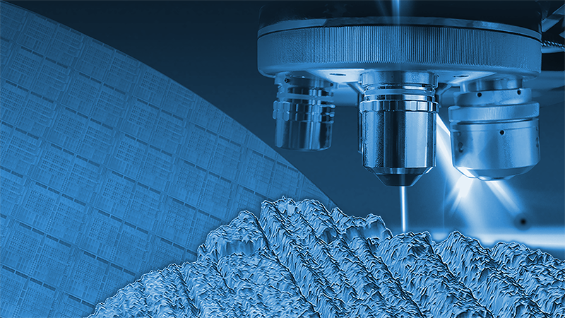
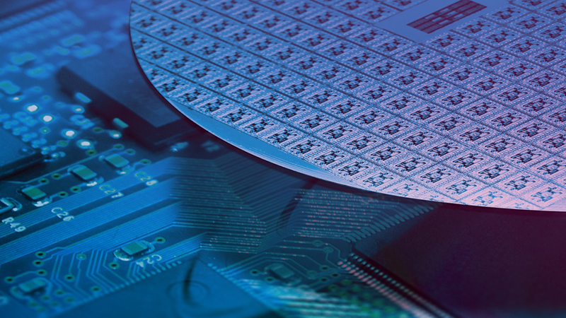
Accelerating Semiconductor Processes Control with Advanced 3D Optical Metrology
Learn how recent advances in 3D Optical Metrology accelerate in-line quality control for both front- and back-end processes
PRESENTATION HIGHLIGHTS:
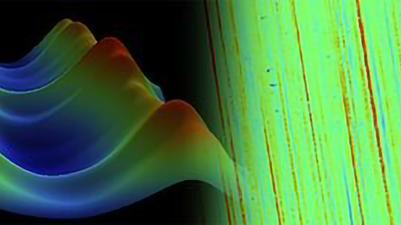
- [00:03:46] Review of non-contact interferometric profiler components, modes, and attributes
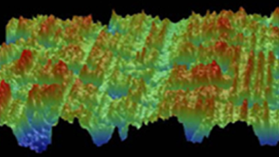
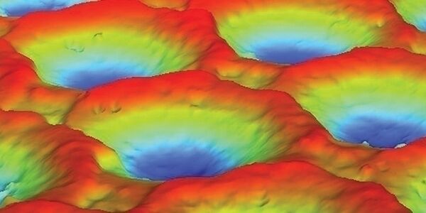
- [00:16:15] Front-end (FEOL) quality control solutions for semiconductor manufacturing
- [00:29:45] Back-end (BEOL) quality control solutions for semiconductor manufacturing
LIVE AUDIENCE Q&A:
- [00:46:43] What lateral resolution can you expect when scanning RDL layers?
- [00:47:53] What is the layer thickness limit for characterization of transparent layers?
- [00:49:06] How do you cope with different refractive indexes or oxide thicknesses for CMP measurements of films?