STEM in SEM Capabilities with Built-in ARGUS Imaging System
Like its predecessor, OPTIMUS 2 detector head has been designed with built-in ARGUSTM system to provide STEM in SEM imaging capabilities. With three Si diodes at its front edge and one Si diode at the center of its screen, OPTIMUS 2 provides:
- Dark Field (DF)-like imaging
- Bright Field (BF)-like imaging while in TKD mapping position
- Imaging at speeds of up to 125,000 pixels/sec
- Fully automatic signal optimization to create images with unequalled quality and detail
The new BF-like imaging capability is particularly useful for drift correction during mapping as well as for near real-time visualization of samples during dynamic experiments like in-situ tensile testing, heating, and electrical biasing of electron transparent samples.

DF-like & BF-like Images Acquired from Various Materials


STEM in SEM Analysis with eWARP TKD
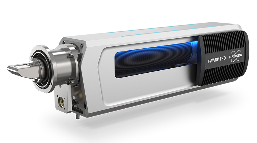
This webnote discusses STEM in SEM analysis using our legacy TKD solution, the eFlash FS detector equipped with an OPTIMUS 2 detector head and ARGUS, which has now been replaced by our next-generation eWARP TKD detector for ultra-fast, high-resolution transmission kikuchi diffraction.
The hybrid pixel sensor technology of the new eWARP provides on-chip binning capability enabling live BF/DF imaging for focusing directly in ESPRIT for best analysis results. Furthermore, eWARP's newly designed pixel array sensor renders the FSD diodes, used on conventional EBSD detectors, redundant, reducing detector complexity, increasing reliability and freeing up space in the vicinity of the sample/stage.