Stylus and Optical Profilometry Webinars

Stylus Profiling Metrology for Soft Matter: Film Thickness and Depth for Flexible Electronic and Microfluidic Devices

Learn more about advanced stylus profiler techniques as Samuel Lesko, Director of Technology and Application Development, Bruker, demonstrates how to collect accurate and repeatable thickness and depth measurements of fragile thin film surfaces


Explore the most innovative capabilities of advanced stylus profilers.

This webinar focuses on how advanced stylus profiler techniques provide effective thickness metrology for fragile thin film surfaces, allowing researchers to both quantify progress and optimize materials and products.


Viewers can expect to gain new insight into:

  • Why advanced stylus profiler techniques provide an optimal thickness metrology solution for thin films;
  • The benefits and advantages of using advanced surface profilometry for thin film analysis; and
  • The range of nanometer- to millimeter-scale thickness metrology applications made possible by advanced surface profiler techniques and instrumentation.


Find out more about the technology featured in this webinar or our other solutions for thin film thickness and depth measurement:

Recorded October 26, 2021 and November 17, 2021

Controlling the Thickness Profile of Thin Films with Advanced Stylus Profilometry

Driven by automation for production, inter-connectivity demands and energy harvesting, Internet of Things (IoT) and green energy solutions are booming. Researchers from both academia and industries actively seek new processes as well as novel materials to develop light and low-cost flexible electronics, or self-power driven and recyclable sensors. Recent innovative devices notably contain stacks of multi-layer thin films with new alloy organic and/or intermetallic materials that are extremely fragile.

By its principle, stylus profiling already ensures unbiased topography even with transparent layers or a different refractive index.

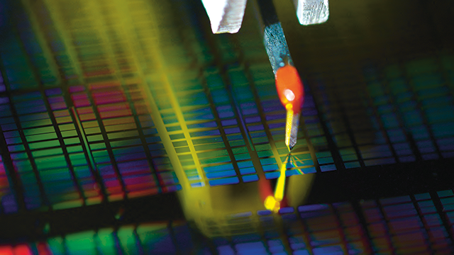
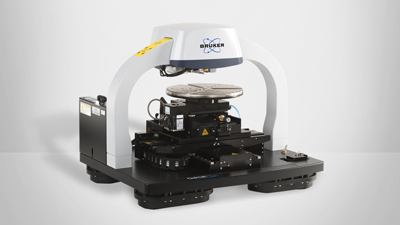
The presentation showcases how advanced stylus profiling further extends to fragile surfaces such as PEDOT:PSS photovoltaic materials, PDMS microfluidic channels or amorphous-indium-gallium-zinc-oxide (IGZO) transistors. A successful solution relies on precise and low controlled force keeping topography unchanged while retaining sub-nanometer repeatability. Through these attributes, the DektakXT stylus profiler opens a wider range of applications for thickness metrology, from nanometers to millimeters.

Featured Products and Technology

Speaker

Samuel Lesko, Ph.D.
Dir. of Technology and Apps Development for Tribology, Stylus & Optical Profilers, Bruker


Samuel Lesko has over 20 years of optical and stylus profiler applications experience, particularly in using white-light interferometry in a wide variety of fields, from MEMS and semiconductor to automotive and aerospace. He is a member of SME and part of ISO/TC 213/WG committee (areal roughness) and obtained his physics Ph.D. and material science engineering degree at the University of Burgundy in France.
Input value is invalid.
FREE TO ACCESS | WATCH ANYTIME

Submit the Form for Instant, Full-Length Access


Measure the thickness and depth of fragile thin film surfaces using advanced stylus profiler techniques.

This webinar focuses on how advanced stylus profiler techniques allow researchers to not only quantify progress but also optimize materials and products.

Viewers can expect to:

  • Learn how researchers use stylus profilers and the practical considerations for using stylus profilometry techniques in their research;
  • Understand how to choose an appropriate technique for thickness measurements of flexible electronics and microfluidics; and
  • See how effective stylus profilers are and how to ensure measurements of soft matter are accurate.


Please enter your first name
Please enter your last name
Please enter your e-mail address
Please enter a valid phone number
Please enter your Company/Institution
What best describes your current interest?
Please add me to your email subscription list so I can receive webinar invitations, product announcements and events near me.
Please accept the Terms and Conditions

             Privacy Notice   Terms of Use


* Please fill out the mandatory fields.

Note: You will be redirected to the webinar viewing page after form submission. After a few moments, you should also receive an email at the address provided that contains a link to re-access the webinar viewing page.

Thank you. Your on-demand video is now available.


DNA-PAINT is a localization-based super-resolution method offering molecular resolution (< 5 nm) combined with unlimited multiplexing capabilities. DNA-PAINT reagents from Massive Photonics are a perfect match for the Bruker Vutara VXL microscope. In combination with the Bruker fluidic system, automated, multiplexed cellular imaging in 3D is now accessible out of the box.

Watch the webinar for practical guidance for DNA-PAINT sample preparation, image acquisition, and data analysis, as well as an introduction to:

  • The Vutara VXL super-resolution microscope and integrated fluidics unit;
  • The theoretical background of DNA-PAINT; and
  • The products available from Massive Photonics for DNA-PAINT experiments.


If you have any questions about these or any of our other products or services, please contact us. Follow @BrukerFM on Twitter for event, product, and webinar updates.