
Stylus Profiling Metrology for Soft Matter: Film Thickness and Depth for Flexible Electronic and Microfluidic Devices
Explore the most innovative capabilities of advanced stylus profilers.
In this webinar, stylus profilometry expert Samuel Lesko, PhD, discusses how stylus profilers can be used to characterize a wide range of soft and thin materials crucial for flexible electronics and microfluidic devices.
Viewers can expect to gain new insight into:
- Why advanced stylus profiler techniques provide an optimal thickness metrology solution for thin films;
- The benefits and advantages of using advanced surface profilometry for thin film analysis; and
- The range of nanometer- to millimeter-scale thickness metrology applications made possible by advanced surface profiler techniques and instrumentation.
Webinar Summary
Driven by automation for production, inter-connectivity demands and energy harvesting, Internet of Things (IoT) and green energy solutions are booming. Researchers from both academia and industries actively seek new processes as well as novel materials to develop light and low-cost flexible electronics, or self-power driven and recyclable sensors. Recent innovative devices notably contain stacks of multi-layer thin films with new alloy organic and/or intermetallic materials that are extremely fragile.
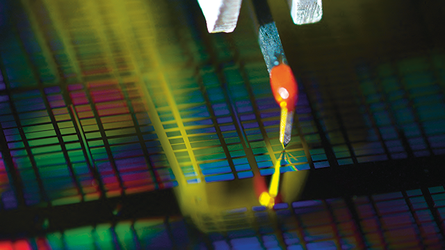
In this webinar, Samuel Lesko, PhD, showcases how advanced stylus profiling further extends to fragile surfaces such as PEDOT:PSS photovoltaic materials, PDMS microfluidic channels or amorphous-indium-gallium-zinc-oxide (IGZO) transistors. He shows an example of PDMS microfluidic structures, where the stylus is aligned using optical videos and motorized feeders to achieve reproducible nanometer-level results even on soft, sticky surfaces.
Find out more about the technology featured in this webinar or our other solutions for thin film thickness and depth measurement:
This resource is included in our Stylus Profiler-Based Characterization of Thin Films knowledge pack.
Get instant access to all app notes, webinars and lectures, and technical demonstrations on using stylus profilometry for thin film characterization, all in one place.

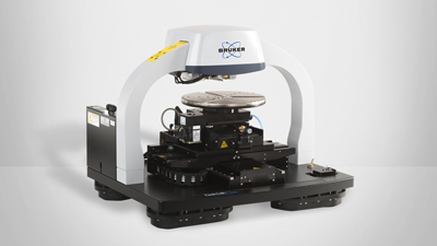
Featured Products and Technology

Speaker

Samuel Lesko, Ph.D.
Dir. of Technology and Apps Development for Tribology, Stylus & Optical Profilers, Bruker
Samuel Lesko has over 20 years of optical and stylus profiler applications experience, particularly in using white-light interferometry in a wide variety of fields, from MEMS and semiconductor to automotive and aerospace. He is a member of SME and part of ISO/TC 213/WG committee (areal roughness) and obtained his physics Ph.D. and material science engineering degree at the University of Burgundy in France.