
Transform Challenging EDS Measurements into Routine Analytical Work
XFlash® FlatQUAD’s unmatched sensitivity and speed makes difficult EDS easy
Elemental analysis with Energy Dispersive X-ray Spectroscopy (EDS or EDX) in Scanning Electron Microscopy (SEM) can be challenging when dealing with complex and difficult samples. These samples include beam-sensitive materials, life science and biological thin sections, semiconductor devices, battery materials, FIB/TEM lamellae, nanoparticles, and samples with topographic features or heavy surface charge accumulation (i.e. glass and ceramics). For such materials, large area EDS detectors (>100 mm2) are preferred, however their inclined detector geometry and small collection angle can hinder efficient signal collection. This results in noisy EDS maps with poor spectral data quality.
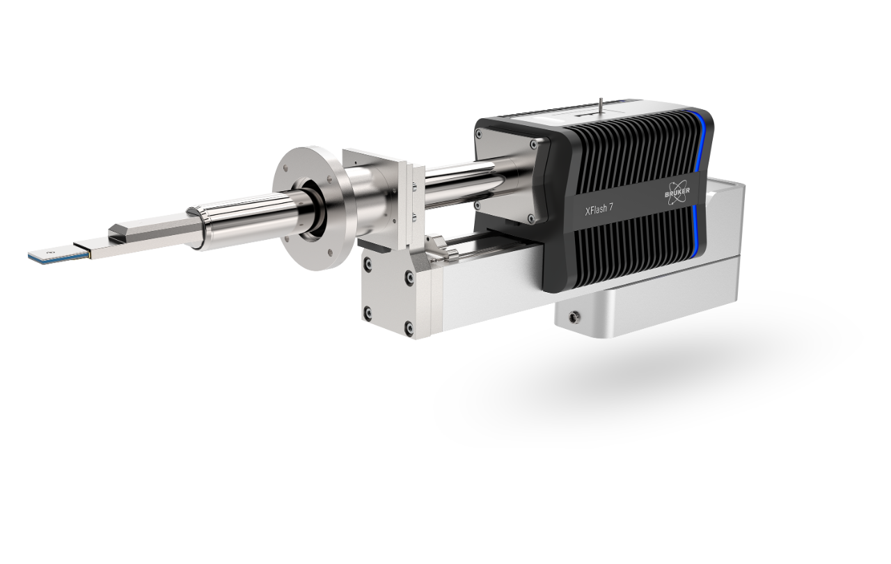
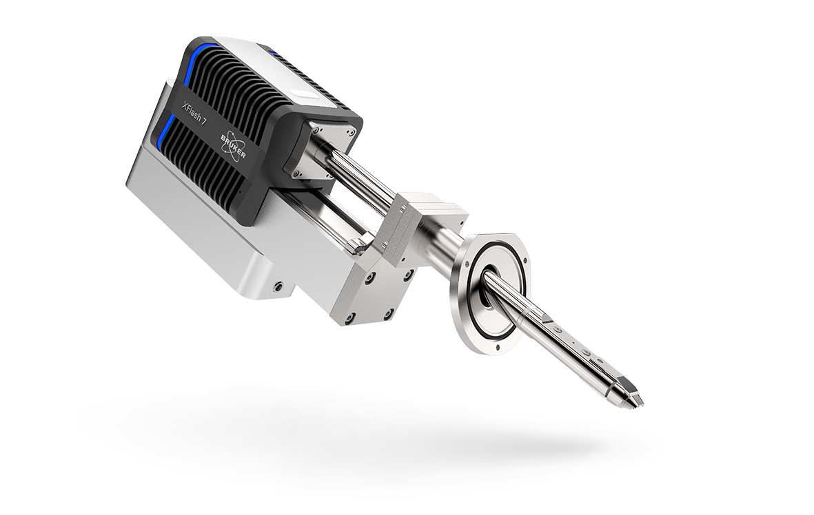
In this webinar, you will learn how the XFlash® FlatQUAD detector can transform your SEM EDS elemental analysis from slow, difficult, and sometimes impossible - to an easy routine analysis. Maximum signal collection is ensured by the detector’s annular four segment SDD design, detector placement under pole-piece, and the high take-off angle. XFlash® FlatQUAD enables unmatched sensitivity, even at low (<3 kV) or high (>15 kV) voltages and ultra-low probe currents (<50 pA). These beam conditions are necessary for “difficult” samples" and are impossible to achieve using conventional single or even multiple large-area EDS detectors with an inclined geometry.
Join us for an informative 30-minute session, where Bruker Nano Analytic’s experts will discuss the capabilities of qualitative and quantitative EDS using the cutting-edge XFlash® FlatQUAD. Discover how this groundbreaking detector can effortlessly handle even the most challenging samples at unparalleled speed (10x – 50x faster) while maintaining unmatched sensitivity, making it is the preferred choice of SEM EDS analysts.
What you will learn:
- Why chemical maps with EDS/EDX in SEM and FIB-SEM are often noisy with no useful data.
- The limitations of conventional large-area EDS detectors for elemental analysis of “difficult” samples in SEM.
- How to overcome common challenges such as surface charge accumulation, shadowing, low signal counts, low X-ray yield, high noise levels, and long measurement times.
- Techniques for the elemental mapping of uncoated samples without using low pressure/low vacuum conditions.
- Practical applications in various fields including life sciences, semiconductors, materials science, geology, and battery research.
- The key features and benefits of EDS using XFlash® FlatQUAD: the 4-SDD segment, BSE-like horizontal insertion EDS detector.
Who should attend?
- Researchers, students, and industry professionals involved in scanning electron microscopy and related fields.
- SEM and TEM users interested in the characterization of nanostructured materials.
- Everyone that is interested in qualitative and quantitative elemental analysis for materials science, life science, semiconductors, and battery materials.
Speakers
Dr. Purvesh Soni
Sr. Applications Scientist EDS, Bruker Electron Microscope Analyzers
Dr. Igor Németh
Application Scientist EDS, Bruker Nano Analytics
Watch the Recording of this Webinar
Please enter your details below to gain access to the recording of this webinar.
