FilmTek 6000 PAR-SE Robotic

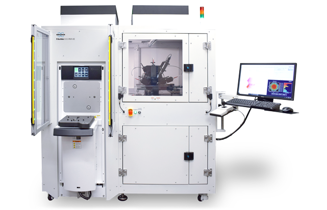
FilmTek 6000 PAR-SE Robotic
The FilmTek™ 6000 PAR-SE combines patented Multi-Angle Differential Polarimetry (MADP) and Differential Power Spectral Density (DPSD) technology to independently measure film thickness and index of refraction. By independently measuring index and thickness, the FilmTek 6000 PAR-SE is far more sensitive to changes in films, particularly films within multi-layer stacks, than existing metrology tools that rely on conventional ellipsometry and reflectometry techniques. This is ideal for both ultra-thin and thick multi-layer film stacks used in forming complex device structures.
Measurement Capabilities
Enables simultaneous determination of:
- Multiple layer thicknesses
- Indices of refraction [ n(λ) ]
- Extinction (absorption) coefficients [ k(λ) ]
- Energy band gap [ Eg ]
- Composition (e.g., %Ge in SiGex, % Ga in GaxIn1-xAs, %Al in AlxGa1-xAs, etc.)
- Surface roughness
- Constituent, void fraction
- Crystallinity/Amorphization (e.g., of Poly-Si or GeSbTe films)
- Film gradient
System Components
Standard:
- Spectroscopic ellipsometry with rotating compensator design (295 nm - 1700 nm)
- Multi-angle, polarized spectroscopic reflection (190 nm - 1700 nm)
- Measures film thickness and index of refraction independently
- Multi-Angle Differential Polarimetry (MADP) technology with SCI’s patented Differential Power Spectral Density (DPSD) technology
- Ideal for measuring ultra-thin films (0.03 Å repeatability on native oxide)
- Patented parabolic mirror technology – small spot size measures within a 50×50 µm feature
- Cassette to cassette wafer handling
- Pattern recognition (Cognex)
- FOUP or SMIF compatible
- SECS/GEM
- Advanced material modeling software
- Bruker's generalized material model with advanced global optimization algorithms
Typical Application Areas

Front End Semiconductor
Perform fast, accurate, and repeatable multi-layer film thickness and refractive index measurements on patterned device wafers for front end semiconductor manufacturing.
FilmTek systems enable process control of oxides, nitrides, ONO, Oxide / Nitride / Cu, polysilicon / oxide, AlN, TaN, TiN, SiGex and composition control, resist, Si3N4/GaAs, ARC, gate oxide, and GaAs films, CMP on Cu, and many other materials encountered throughout the entire wafer fabrication process.
Technical Specifications
| Film Thickness Range | 0 Å to 150 µm |
|---|---|
| Film Thickness Accuracy | ±1.0 Å for NIST traceable standard oxide 100 Å to 1 µm |
| Spectral Range | 190 nm - 1700 nm (220 nm - 1000 nm is standard) |
| Measurement Spot Size | 50 µm |
| Sample Size | 2 mm - 300 mm (150 mm standard) |
| Spectral Resolution | 0.3 nm - 2nm |
| Light Source | Regulated deuterium-halogen lamp (2,000 hrs lifetime) |
| Detector Type | 2048 pixel Sony linear CCD array / 512 pixel cooled Hamamatsu InGaAs CCD array (NIR) |
| Computer | Multi-core processor with Windows™ 10 Operating System |
| Measurement Time | ~2 sec per site (e.g., oxide film) |
Performance Specifications
| Film(s) | Thickness | Measured Parameters | Precision (1σ) |
|---|---|---|---|
| Oxide / Si | 0 - 1000 Å | t | 0.03 Å |
| 1000 - 500,000 Å | t | 0.005% | |
| 1000 Å | t , n | 0.2 Å / 0.0001 | |
| 15,000 Å | t , n | 0.5 Å / 0.0001 | |
| 150.000 Å | t , n | 1.5 Å / 0.00001 | |
| Nitride / Si | 200 - 10,000 Å | t | 0.02% |
| 500 - 10,000 Å | t , n | 0.05% / 0.0005 | |
| Photoresist / Si | 200 - 10,000 Å | t | 0.02% |
| 500 - 10,000 Å | t , n | 0.05% / 0.0002 | |
| Polysilicon / Oxide / Si | 200 - 10,000 Å | t Poly , t Oxide | 0.2 Å / 0.1 Å |
| 500 - 10,000 Å | t Poly , t Oxide | 0.2 Å / 0.0005 |
How Can We Help?

Bruker partners with our customers to solve real-world application issues. We develop next-generation technologies and help customers select the right system and accessories. This partnership continues through training and extended service, long after the tools are sold.
Our highly trained team of support engineers, application scientists and subject-matter experts are wholly dedicated to maximizing your productivity with system service and upgrades, as well as application support and training.