FilmTek 2000 PAR-SE
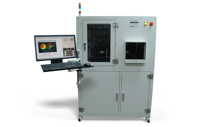

FilmTek 2000 PAR-SE
The FilmTek™ 2000 PAR-SE spectroscopic ellipsometry/multi-angle reflectometry system combines cutting-edge and proprietary FilmTek technologies to deliver industry-leading accuracy, precision, and versatility for nearly any advanced thin film measurement application from R&D to production. Its standard small spot measurement size and pattern recognition capabilities make this system ideal for characterizing patterned films and product wafers.
Part of our most advanced combined metrology product line ("PAR-SE"), FilmTek 2000 PAR-SE is uniquely able to fulfill measurement requirements outside the average thickness, resolution, and spectral ranges needed for mainstream applications and provided by standard instrumentation.
It provides exceptionally precise and repeatable thickness and refractive index measurements on ultra-thin to thin films (particularly those within multilayer stacks). Moreover, this system is far more sensitive to non-uniformity in these samples than conventional ellipsometry and reflectometry tools. This is the result of FilmTek 2000 PAR-SE's multimodal design, which combines high-performance rotating compensator-based spectroscopic ellipsometry with our patented Multi-Angle Differential Polarimetry (MADP) and Differential Power Spectral Density (DPSD) technology, extended/wide spectral range DUV multi-angle polarized reflectometry, our patented parabolic mirror optical design, and advanced Filmtek software.
Measurement Capabilities
Enables simultaneous determination of:
- Multiple layer thicknesses
- Indices of refraction [ n(λ) ]
- Extinction (absorption) coefficients [ k(λ) ]
- Energy band gap [ Eg ]
- Composition (e.g., %Ge in SiGex, % Ga in GaxIn1-xAs, %Al in AlxGa1-xAs, etc.)
- Surface roughness
- Constituent, void fraction
- Crystallinity/Amorphization (e.g., of Poly-Si or GeSbTe films)
- Film gradient
System Components
Standard:
- Spectroscopic ellipsometry with rotating compensator design (295 nm - 1700 nm)
- Multi-angle, polarized spectroscopic reflection (190 nm - 1700 nm)
- Measures film thickness and index of refraction independently
- Multi-Angle Differential Polarimetry (MADP) technology with SCI’s patented Differential Power Spectral Density (DPSD) technology
- Ideal for measuring ultra-thin films (0.03 Å repeatability on native oxide)
- Camera for imaging measurement location
- Pattern recognition
- 50 micron spot size
- Advanced material modeling software
- Bruker's generalized material model with advanced global optimization algorithms
Optional:
- Generalized ellipsometry (4×4 matrix generalization method) for anisotropy measurements (nx, ny, nz)
- Cassette to cassette wafer handling
- FOUP and SMIF compatible
- Pattern recognition (Cognex)
- SECS/GEM
Typical Application Areas
Virtually all translucent films ranging in thickness from less than 1 Å to approximately 150 µm can be measured with high precision. Typical application areas include:
- Silicon semiconductor
- Compound semconductor
- LED/OLED
With flexible hardware and software that can be easily modified to satisfy unique customer requirements, particularly in R&D and production environments.
Technical Specifications
| Film Thickness Range | 0 Å to 150 µm |
|---|---|
| Film Thickness Accuracy | ±1.0 Å for NIST traceable standard oxide 100 Å to 1 µm |
| Spectral Range | 190 nm - 1700 nm (220 nm - 1000 nm is standard) |
| Measurement Spot Size | 25 µm - 300 µm (normal incidence); 2 mm (70°) |
| Sample Size | 2 mm - 300 mm (150 mm standard) |
| Spectral Resolution | 0.3 nm - 2nm |
| Light Source | Regulated deuterium-halogen lamp (2,000 hrs lifetime) |
| Detector Type | 2048 pixel Sony linear CCD array / 512 pixel cooled Hamamatsu InGaAs CCD array (NIR) |
| Automated Stage with Auto Focus | 300 mm (200 mm is standard) |
| Computer | Multi-core processor with Windows™ 10 Operating System |
| Measurement Time | <1 sec per site (e.g., oxide film) |
Performance Specifications
| Film(s) | Thickness | Measured Parameters | Precision (1σ) |
|---|---|---|---|
| Oxide / Si | 0 - 1000 Å | t | 0.03 Å |
| 1000 - 500,000 Å | t | 0.005% | |
| 1000 Å | t , n | 0.2 Å / 0.0001 | |
| 15,000 Å | t , n | 0.5 Å / 0.0001 | |
| 150.000 Å | t , n | 1.5 Å / 0.00001 | |
| Nitride / Si | 200 - 10,000 Å | t | 0.02% |
| 500 - 10,000 Å | t , n | 0.05% / 0.0005 | |
| Photoresist / Si | 200 - 10,000 Å | t | 0.02% |
| 500 - 10,000 Å | t , n | 0.05% / 0.0002 | |
| Polysilicon / Oxide / Si | 200 - 10,000 Å | t Poly , t Oxide | 0.2 Å / 0.1 Å |
| 500 - 10,000 Å | t Poly , t Oxide | 0.2 Å / 0.0005 |