In-situ SEM Nanomechanics with Scanning Probe Microscopy Imaging
Bruker’s industry-leading Hysitron® scanning probe microscopy (SPM) is now available for in-situ scanning electron microscopy (SEM) with the Hysitron PI 89 SEM PicoIndenter. By utilizing piezo-actuated scanning stages in closed-loop control with the transducer, the tip can be rastered relative to the sample rapidly with nanoscale precision. This enables topographical imaging of sample surface based on the force feedback.
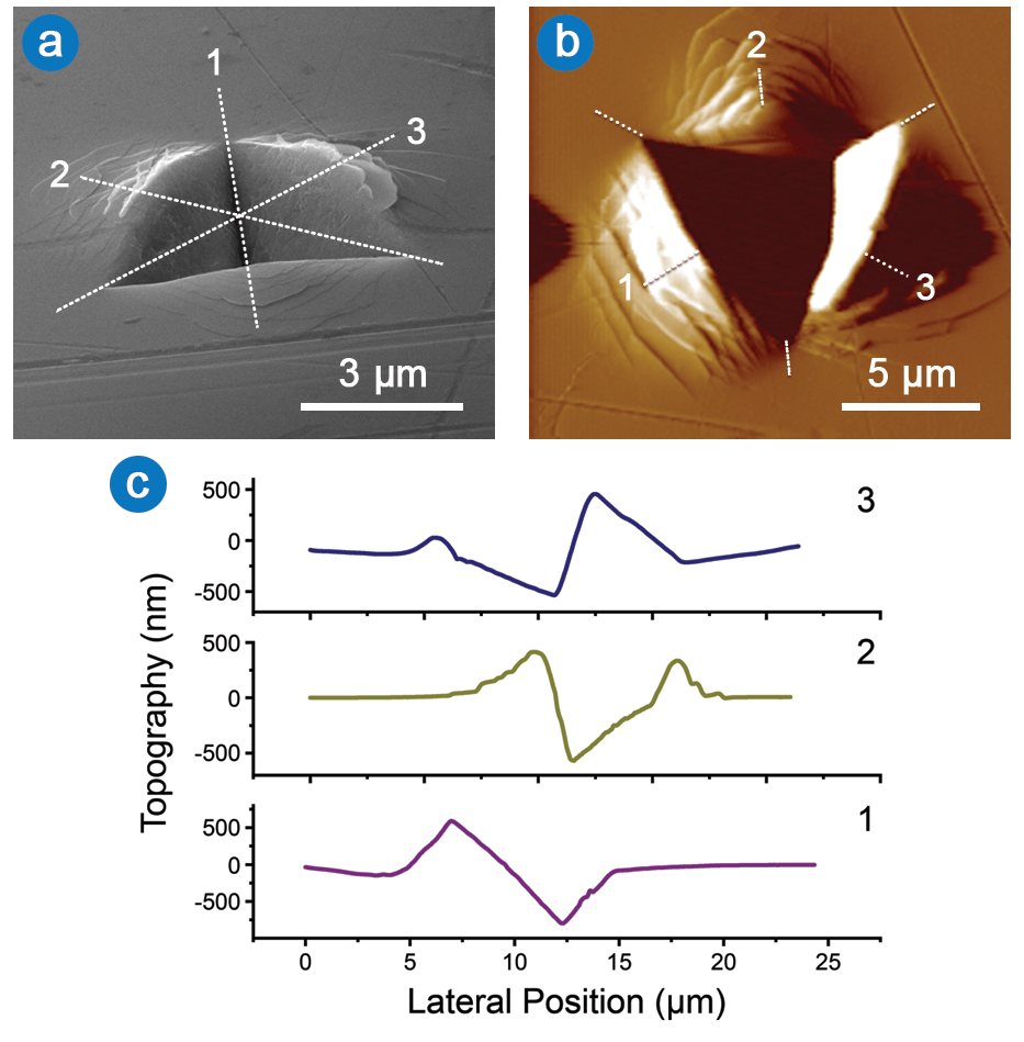
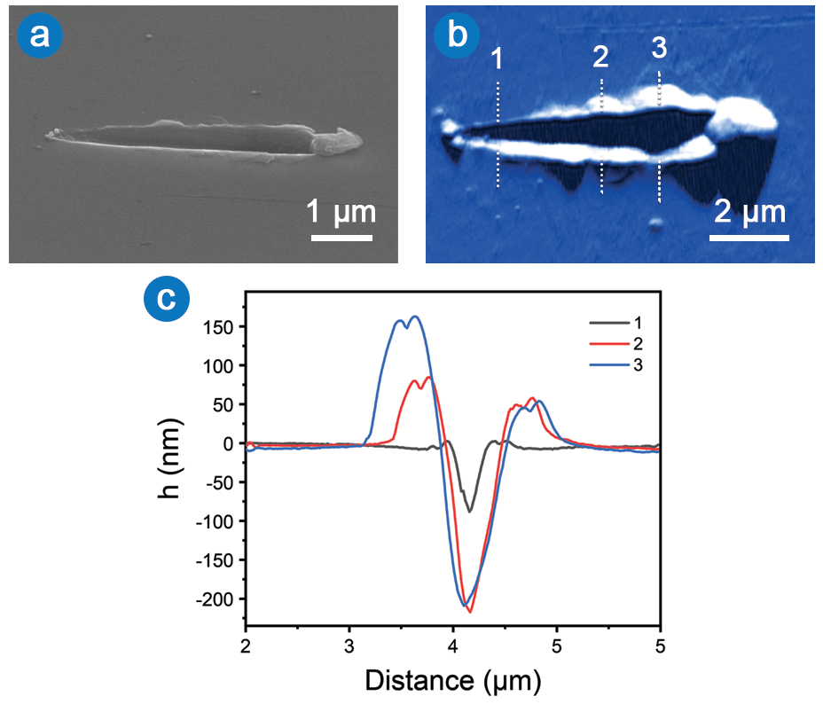
Even though surface features can be viewed in high-resolution with secondary electron imaging in the SEM, obtaining quantitative topographical data is challenging. SPM can address this issue by using the same probe to image the sample surface as is used to perform the indentation testing. This provides accurate height information of sample features, as well as related parameters such as surface roughness. This capability is also particularly useful for analyzing post-test deformation, such as measuring pile-up or sink-in from nanoindentation and scratch tracks.