Passivation Layers
What is a Passivation Layer?
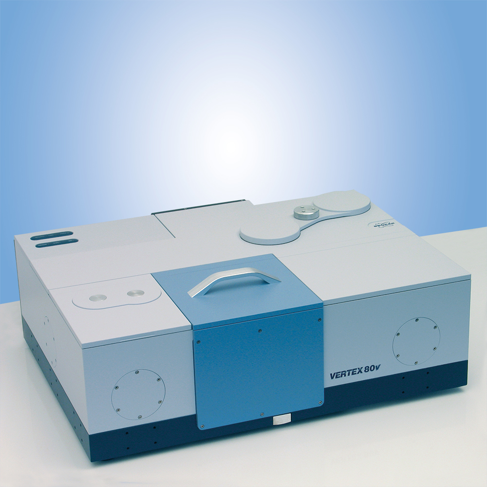
Passivation layers on semiconductors play an important role and serve as e.g. protection, electronic isolation or antireflectance layer. Bruker FT-IR research spectrometers are the ideal tools for the fast, sensitive and non-destructive analysis of such passivation layers.
Using FT-IR for Passivation Layer Analysis
Various sample/wafer holders are available for transmittance, reflectance or ATR measurement modes to investigate passivation layers of different thickness.
E.g. Boron and Phosphorous Phosphosilicate glass (PSG) and Boronphosphosilicate glass (BPSG) can be characterized and quantified with transmittance measurement in mid IR region, using a suitable calibration.
Dedicated wafer mapping accessories for the research series FT-IR spectrometers allow for the automated acquisition of reflectance and transmittance spectra at different sample positions.
It can perform e.g. simultaneously layer thickness evaluation and quantitative analysis of BPSG layers and has been well accepted in QC. Even ultrathin layers like SiN plasma layers, ultra-low k layers or self-assembled monomolecular layers on single crystal silicon can be analyzed with highest sensitivity thanks to Bruker’s innovative wafer ATR accessory. Want to know more?