Polymers Research
Due to their robust, environmentally friendly and cost-effective nature over other materials, polymers have become ubiquitous in research and manufacturing. Polymeric surfaces present in-homogeneities in microscopic scale, which can affect their properties of adhesion, wettability, abrasion and degradation in the environment, which has allowed them to be customized to suit a very wide range of uses. Atomic force microscopy has become a preferred technique for characterizing polymers. Some advantages are that it is not necessary to use vacuum during analysis or conductive covering on the samples; as well as the capability to direct measure height and roughness with atomic resolution. In addition, the AFM technique does not demand prior complex treatment of the sample for the characterization of the morphology, microstructure and crystallinity of different polymer films.
Bruker AFMs enable nondestructive, in situ imaging of polymers with nanometer resolution with TappingMode (compositional mapping, fast scanning of dynamic behavior) and proprietary PeakForce Tapping® (highest resolution imaging, quantitative property mapping). These and other nanoscale characterization techniques cover the full range of structural length scales:
- Molecular arrangement/defects
- Fibrils, lamellae, brushes
- Interphases, phase-separated domains

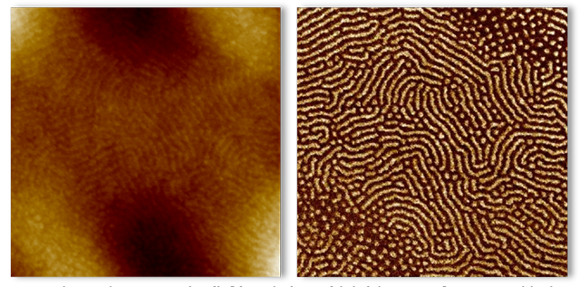
High-Resolution Compositional Mapping
Nanoscale distribution of components or multi-phases is critical to polymer function. Physical AFM tip-sample interaction enables simultaneous detection of multiple sample properties. TappingMode phase imaging provides qualitative compositional mapping based on differences in material properties. Bruker's AFMs enable detailed characterization of:
- Amorphous, crystalline, mesomorphic regions
- Nanodomains in polymer blends
- Phase-separated copolymers
- Nanofillers in polymer composites
In Situ Studies of Dynamic Behavior and Processes
Polymer dynamics range from intrinsic thermal behavior to interactions with the environment. Direct observation of structural changes can provide insights into key mechanisms and kinetics governing:
- Crystallization/melting
- Degradation/decomposition
- Chain and brush ordering
- Lamellae formation
The tip-scanning FastScan AFM enables high-speed TappingMode imaging of dynamic behavior in real-time and real-space, independent of sample size and environment.
Nanoscale Imaging of Challenging Polymer Structures
Certain polymer features, such as brush structure, chain-packing, and molecular/point defects, are difficult to image. Direct control of imaging force is critical to resolving these molecular and mesoscale structures. PeakForce Tapping enables <100 pN force control for highest resolution imaging, even on the smallest, most challenging samples. Since this technology maps mechanical properties simultaneously with topography, a comprehensive understanding is much easier to achieve with this proprietary technology.

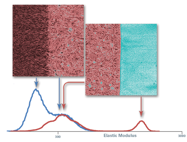
Quantitative Elastic Modulus Mapping
Mechanical performance of polymer materials critical to:
- Optimizing formulation/blends
- Managing processing conditions
- Evaluating product lifetime
Microscopic organization requires characterization of Young’s modulus and stiffness at interphases/interfaces. PeakForce QNM® provides out-of-the-box quantitative elastic modulus mapping with nanometer resolution, enabling researchers to more easily and efficiently characterize polymers.
Quantitative Viscoelasticity Measurements
Viscoelastic properties of polymers are central to many commercial applications, ranging from vibration isolation and noise damping to shock absorption, dirt-resistant coatings, and temperature-dependent requirements. Macroscale properties are governed by nanoscale structure, for example, interphases, interfaces, and domains. Time-temperature superposition is needed to fully understand viscoelastic behavior.
Bruker's AFM-nDMA mode provides fully quantitative viscoelastic property mapping, including storage and loss modulus, as well as loss tangent (separate from adhesion). Rheological temperature and frequency ranges enable mastercurve construction at nanoscales.

Molecular Conductivity Mapping of Organic Semiconductors
Conductive polymers are used in many electronic applications (e.g., organic photovoltaics). Charge transport properties and carrier mobilities of organic semiconductors are directly related to level of structural order. The ability to map conductive pathways over multiple length scales is key to improving efficiency. PeakForce-TUNA enables molecular-resolution, quantitative conductivity maps without damaging delicate samples. With this technology, researchers can now directly and reliably correlate topography and nanomechanical properties.