
Cutting Edge Imaging: Harnessing Diamond Probes for Advanced AFM Performance
Diamond probes enhance AFM precision, throughput, and lifetime
Diamond‑based AFM probes are redefining what is possible in nanoscale characterization, enabling researchers and engineers to push the limits of resolution, durability, and multifunctional measurement. This webinar brings together three experienced AFM specialists to showcase the value of modern diamond probe technologies.
Join us for this webinar to learn about:
- Unique material advantages of diamond probes
- Probe types engineered for high-resolution topography and persistent sharpness
- Electrical imaging and analysis with conductive diamond probes
- Cutting-edge application-driven use cases for diamond probes
Webinar Summary
Diamond‑based AFM probes add immense value for advanced scientific and industrial workflows. This webinar features three experienced AFM specialists—Ian Armstrong, Peter De Wolf, and Hector Cavazos—who will cover:
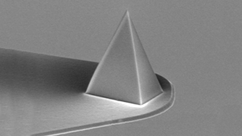
- Unique material advantages of diamond probes, including exceptional hardness, chemical inertness, conductivity options, and long‑term wear resistance. These properties make diamond‑tipped probes uniquely suited for demanding applications in which conventional silicon or metal-coated silicon probes rapidly degrade or lose fidelity.
- Probe types engineered for high-resolution topography and persistent sharpness, emphasizing how diamond tips maintain imaging quality over rough or abrasive surfaces. Data examples will highlight the consistent performance of diamond probes in roughness quantification, long‑duration wear studies, and high‑speed scanning scenarios.
- Electrical imaging and analysis with conductive diamond probes. Diamond’s conductivity and robustness support stable, repeatable electrical characterization—even under high contact forces. Examples demonstrate how conductive diamond probes excel in techniques such as scanning spreading resistance microscopy (SSRM), TUNA-style current mapping, and nanoscale conductivity measurements on challenging materials.
- Cutting-edge application‑driven case studies, including the use of diamond probes in photomask repair, semiconductor defect analysis, and harsh‑environment metrology. Examples will illustrate how the mechanical resilience and multifunctionality of diamond probes enable workflows not feasible with traditional probe materials.
Attendees will leave with practical guidance for selecting and deploying diamond probes to enhance AFM precision, throughput, and lifetime across a broad range of advanced applications.
Find out more about the technology featured in this webinar or our other solutions for Atomic Force Microscopy: