Low-kV Elemental Mapping of Core-Shell Au-Si Nanoparticles
Elemental mapping and imaging of nanostructures with 15 kV scanning transmission electron microscopy (STEM) is achieved with the dedicated solution of Delong’s LVEM 25E electron microscope and Bruker’s XFlash® 7T30 detector for Energy Dispersive Spectroscopy (EDS).
This STEM EDS solution provides the analytical capability to study Au-Si core-shell nanoparticles with a 10 nm core (Fig. 1). Elemental maps show distribution of gold and silicon within individual nanoparticles. Bruker ESPRIT Software’s drift correction ensured reliable elemental mapping, where both Au cores and Si shells are clearly identified with EDS.
A line profile along a single Au-Si core-shell structure precisely highlights the inner structure of a nanoparticle (Fig. 2). The line profile was extracted from the ESPRIT HyperMap data. To properly separate element signals, net intensities were calculated by deconvolution after background subtraction.
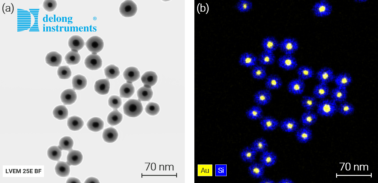
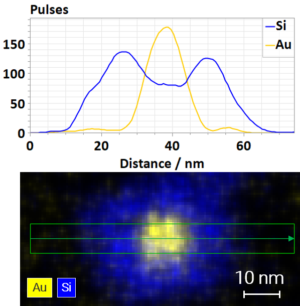
Fig. 2. A line profile (background-subtracted net intensity) extracted from the ESPRIT HyperMap data highlights the inner structure of an individual Au-Si core-shell nanoparticle.