
What is EDS/EDX? Introducing Energy Dispersive
X-Ray Spectroscopy
Energy Dispersive Spectroscopy (EDS) is a popular microanalytical technique that is used to identify and quantify the elements present in a sample. When working alongside a scanning electron microscope (SEM) or scanning transmission electron microscope (STEM), EDS can be used to create elemental maps of samples.
Owing to its popularity EDS has many names - from the more conventional EDS to Energy Dispersive X-ray Spectroscopy (EDX or EDXS) or sometimes even Energy Dispersive Analysis of X-rays (EDAX).
Elemental mapping allows researchers to see their samples in colour - regions of interest that were previously invisible can suddenly become clear, contamination can be spotted, or information can be retrieved that can help develop understanding of the sample's history, formation conditions and macroscopic properties.
These are just a few of the applications of EDS. To find out more about this powerful technique, and what it can be used for, continue reading!

Figure 1: A standard SEM image of a semiconductor feature (left) next to a composite elemental map of the same structure taken using EDS (right).
How Does EDS Work?
EDS works by measuring the energy and intensity of the X-rays that are emitted by a sample when it is exposed to the electron beam of an electron microscope. Depending on if a SEM or TEM is used the technique is called either SEM EDS or TEM EDS.
During EDS anaylsis the microscope's high-energy electron beam interacts with the atoms of the sample. This interaction has many effects, one is the ejection of an atom's inner-shell electron creating an electron vacancy, which is quickly occupied by a higher-energy, outer-shell electron. As the outer-shell electron drops to a lower-level shell it loses energy and this excess energy is emitted as X-rays (figure 2).
The X-rays emitted during this process are called characteristic X-rays because their energies are unique for each element. Detecting and measuring these characteristic X-rays can be used to determine which elements are present in a sample and at what quantity.
The detection and measurement of the emitted X-rays is carried out by a SDD (short for silicon drift detector) and for each pixel of measurement the energies and intensities of the X-rays are recorded. Software and a spectral library are then used to to identify the elements present based on the measured characteristic X-ray energies and their amount based on the respective intensities.

Figure 2a - An incident electron from the SEM electron beam collides with an inner shell electron of an atom in the sample. This results in the emission of an inner core electron, leaving behind an inner shell vacancy.

Figure 2b - An outer shell electron relaxes to occupy the newly created inner shell vacancy. A characteristic X-ray, of energy hv, which is equal to the energy of the electronic transition, is emitted during the relaxation.
What is Elemental Mapping?
Elemental mapping is a technique used to visualize and characterize the spatial distribution of elements within a sample. It provides a detailed representation of how different elements are distributed across the sample's surface allowing users to develop a greater understanding of a samples structure.
Elemental maps are created by the combination of point-by-point elemental information collected during SEM EDS or STEM EDS. In the elemental map, the intensity or color scale represents the concentration of a particular element at each point. High intensities or brighter colors indicate regions with higher concentrations of the element, while low intensities or darker colors represent regions with lower concentrations.
The process behind the creation of an elemental map can be seen in figure 3. This example shows a HyperMap, also known as a spectral image, taken using hyperspectral imaging.
Figure 3: Elemental map taken by EDS SEM with associated spectra for three chosen points in the map. This data was processed using ESPRIT HyperMap software.

Figure 4: Elemental maps taken during EDS SEM, overlaid on a larger SEM image. This particular image is of the nanoscale features on a semiconductor-based FinFET device.
Live Elemental Mapping
Using the latest technology and software it is now possible to map the elements present in a sample in real time via a process called live elemental mapping. This benefits EDS users by improving their workflows, increasing efficiency and helping ensure important features are not overlooked.
Live elemental mapping, using software such as ESPRIT LiveMap, allows users to scan over a sample to identify a region of interest and then, once identified, take higher resolution measurements of interesting features.
Video 1: Live elemental mapping of a failed welding seam. Dynamic elemental mapping allows users to quickly locate a region of interest (ROI) before taking in-depth measurements.
What Type of Detector is Used for EDS?
Almost all modern EDS systems now use a Silicon Drift Detector (SDD). SDDs consist of a disk of silicon, typically a few hundred microns thick, with an intricate electrode structure on its surface. This structure generates an electric field forcing the electrons, created by the X-rays inside the SDD, to move towards the read-out electrode.
Once a X-ray photon, emitted by the sample hits the SDD, it creates electron-hole pairs. The number of created electrons is proportional to the energy of the X-ray. Ideally all electrons drift towards the read-out electrode so that the energy of the X-ray can be measured. The nature of the SDD allows an extremely fast collection of multiple X-rays, which enables ultra-high throughput and fast elemental mapping at high resolutions.
Bruker’s latest generation of EDS detectors, XFlash® 7, are an advanced SDD with several features that make elemental analysis faster and more accurate than ever. Bruker also provides a range of detectors for users who want to obtain the best solid angle possible for increased detector performance.

Figure 7: The XFlash® 7 EDS detector uses a SDD with advanced processing for fast and accurate elemental analysis.
How do Silicon Drift Detectors Work?
A Silicon Drift Detector (SDD) is a semiconductor-based detector used in modern EDS detectors such as the XFlash® 7 series.
SDDs consist of a disk of silicon, a few hundred microns thick, with a complex electrode structure at their surface that induces an electric field in the SDD.
When X-ray photons emitted from the sample to be analyzed interact with the silicon disk in the SDD in the detector, electron-hole pairs are generated there.
The electric field induced by the electrode structure causes the mobile electrons to drift toward a central collecting anode, where the signal is measured as a voltage step.
X-rays with higher energy result in the generation of more mobile electrons and, in turn, a higher signal step - this is shown in the second event in the video.
If the electrons are generated further away from the electrode, the electrons drift apart on their way to the electrode and the voltage step height has the same value but the slope is smaller.
Each individual voltage step caused by one X-ray photon is then sorted into a histogram at a position corresponding to the step height by using a multichannel analyzer. A complete spectrum is formed by many of these signal steps sorted by their energy and is a fingerprint of the sample composition.
The nature of the SDD allows an extremely fast detection of multiple X-rays in a very short time period, enabling ultra-high throughput and therefore fast elemental mapping at high spatial resolutions.
What is the Solid Angle and Why is it Important?

Figure 5: Diagram illustrating the concept of the solid angle.
The solid angle in EDS refers to the angular range over which an EDS detector can collect X-rays emitted from the sample – the solid angle is often described using the steradian, sr, which is a three-dimensional equivalent of a radian.
The solid angle is effectively a measure of the detector's field of view for X-ray detection. Because the solid angle describes how much surface of a sphere around the point of analysis is available for X-ray detection it has a direct impact on a detector’s collection efficiency.
The detector and SEM/TEM geometry is often a factor that must be optimized to increase the solid angle – Bruker’s XFlash® 100oval detectors have a unique oval-shaped geometry that allows EDS to be carried out at a higher solid angle. In addition, the XFlash® FlatQUAD detector sits between the sample and pole piece for measurements at the highest solid angle available.
By working at an increased solid angle users can further expand the possibilities of EDS. In addition to being able to collect more-accurate data at a higher throughput an increased solid angle improves the sensitivity of an EDS measurement, allowing users to carry out an EDS analysis at lower energies. This is particularly useful when analyzing samples that are beam-sensitive, i.e. those that would degrade under high-energy electron beams, such as biological samples and some semiconductors.

Figure 6: High-resolution elemental map of a sea urchin taken using a FlatQUAD detector. Maximization of the solid angle means EDS can be ran at a lower energy, allowing the elemental distribution in delicate biological samples to be mapped.
What Applications is EDS Used For?

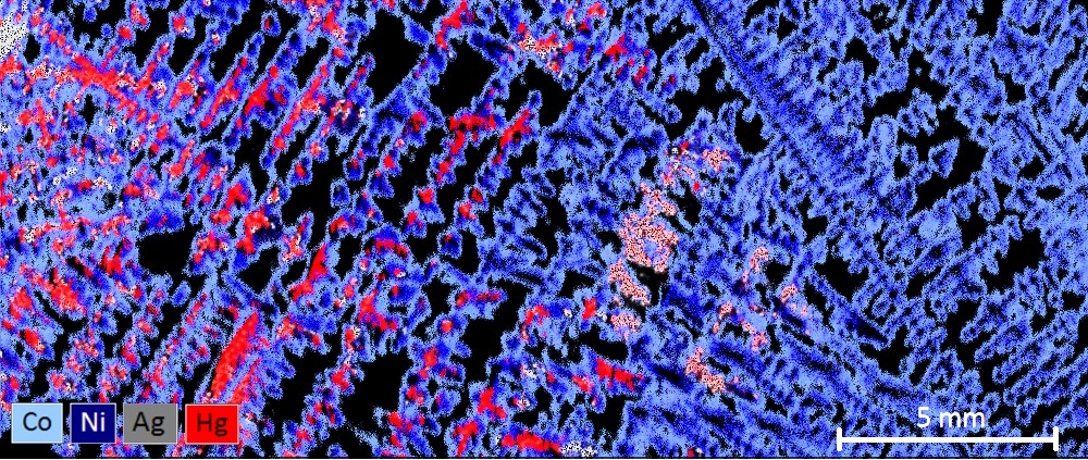
Figure 8: An elemental map of a failed welding seam taken using SEM EDS.
Energy-Dispersive X-ray Spectroscopy (EDS) can be used in many different applications in the scientific and industrial fields.
One significant application area is in the materials sciences. EDS allows users to identify different phases in their materials of interest and to create compositional maps of a diverse range of materials such as metals, alloys, ceramics, and polymers. EDS can be used to examine microstructural features on a sample, to examine surface contamination, and to characterize thin films and coatings. The ability to analyze elemental composition and distribution at high spatial resolution makes EDS invaluable for understanding materials.
In high-tech industries such as the semiconductor and battery industries EDS is an invaluable tool used for both research and development (R&D) and quality control (QC).
EDS allows researchers to see how elements are distributed within the most advanced semiconductor devices and allow for the localized detection of contaminants that may impact device performance. In the battery industry, EDS is employed for characterizing electrode materials, analyzing electrolyte composition, and investigating degradation mechanisms to enhance battery performance and lifespan.
The potential uses for elemental mapping is huge and, as such, EDS can be used in many more applications – from forensics to mineralogy, from archaeology to metallurgy.
Augmenting SEM EDS with More Analytical Capabilities
In addition to systems for EDS Bruker Nano Analytics provides additional systems to add even more analytical capabilities to electron microscopes.
Our Electron Microscope Analyzer range includes systems for:
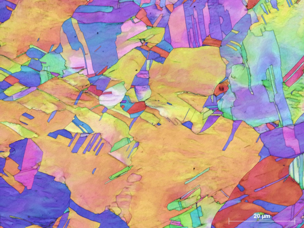
- EBSD (Electron Backscatter Diffraction) - for the analysis of a materials crystallographic structure
- Micro-XRF on SEM - for trace element detection and layer analysis
- WDS (Wavelength Dispersive Spectroscopy) - for elemental mapping with increased analytical precision

Figure 9: The Electron Microscope Analyzer range includes systems for EDS, EBSD, WDS and micro-XRF on SEM.