Increasing the Energy Range and Sensitivity of EDS
Overcome the Limits of Conventional EDS
Energy Dispersive Spectroscopy (EDS) is a powerful technique for elemental analysis using a SEM. Conventional EDS analysis involves measuring the characteristic X-ray energies emitted from a sample when it interacts with the electron beam.
Whilst EDS SEM has many strengths it also has analytical limits, for example, the detectable elemental X-ray energy range is commonly limited to 20 keV (at most) and the sensitivity is limited to approximately 1000 ppm, meaning elemental peaks at low concentrations levels are often lost in the background of electron excitation.
The addition of a micro-XRF source to an SEM EDS system introduces a second excitation source with photons. The focused X-ray beam of the micro-XRF source is far more efficient at generating elemental fluorescence at higher energies, thus yielding elemental peaks up to 40 keV. That makes it possible to detect X-ray line series which are not detectable by electron excitation.
For example, for samples containing transition metals or other high atomic number elements at trace concentrations, the use of an X-ray source coupled with an EDS detector allows users to detect elements that are not observed in the EDS SEM spectrum.
What is Full Range EDS?
Full Range EDS is Bruker's name for analysis using dual excitation of micro-XRF and electron beam sources combined with an EDS detector. The addition of a micro-XRF source (XTrace 2) to a conventional EDS set-up creates a dual-beam system, where samples interact with either the electron beam of the SEM or the X-ray photons from the micro-XRF source, or both.
The combination of the two excitation sources delivers unique additional analytical capabilities with no modification of the EDS detector hardware required. increasing the energy range and sensitivity of EDS detector. This means that higher-energy excitation lines can be detected (i.e. up to 40 keV), and trace elements can be measured down to approximately 10 ppm, element and matrix dependent).

Discover More About Your Sample with Full Range EDS
Full Range EDS delivers a wide range of benefits over conventional EDS, allowing users to discover even more about their sample. This includes the ability to:
- See high energy transitions, including the ability to detect additional elemental line series that are not seen with conventional EDS, especially above 20 keV.
- Detect & quantify elements at trace level concentrations.
- Analyze beam-sensitive and non-conductive samples.
- Visualize topographic samples at high-resolution.
- Gather elemental maps over large areas at micrometer resolution.
- Detect elements and minerals at and below the sample surface.
- Analyze multi-layered systems.
See High-Energy Elemental X-ray Line Series
Full Range EDS enables the detection of higher energy excitations that are induced in the sample being analyzed.
This means higher energy lines, such as K lines from elements such as Ag (22.1 keV), Sn (25.3 keV), or Ba (32.2 keV) are now detectable as shown in the adjacent spectrum for La (33.4 keV).


The periodic tables below show the typical elemental lines which can be detected using conventional EDS with an electron beam excitation source (left) and the elemental lines which can be detected using Full Range EDS (right).
For example, when using conventional EDS to analyze Tin (Z = 50), normally only the M Lines (at 0.4keV) and the L lines (at 3.4 keV) can be detected, whereas with Full Range EDS, the K lines (at 25.3 keV) are also detectable.
The majority of peak overlaps occur in the low energy region of the spectrum and not in the high energy region. The ability to detect the high energy K-lines allows users to more confidently determine if an element is truly present in a sample.
Differences in Detectable Elemental Line Series for Electron Beam and X-ray Excitation


Detect Trace Elements
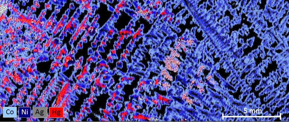
Many elements are not detectable at low concentrations with conventional EDS because their X-ray signal is typically lost in the background. Bruker’s Full Range EDS solution makes it possible to detect those trace level signal down to even 10 ppm (element and matrix dependent) since micro-XRF excitation yields a spectrum that has a much lower spectral background.
The periodic table below shows the detection limits for various elements achievable with Full Range EDS. For the elements marked in light orange, concentrations down to even 5 ppm can be detected, which are not achievable by conventional EDS.


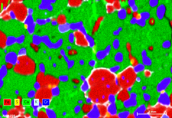
Analyze Beam-Sensitive or Non-Conductive Samples
Full Range EDS allows users to analyze delicate non-conductive and beam sensitive samples without the need to coat their samples as the photons from the x-ray beam do not charge the samples. This makes Full Range EDS a universal package to characterize a wide variety of sample types in the SEM.
Solid samples, powders and even beam-sensitive samples can be measured using Full Range EDS without time consuming sample preparation work.


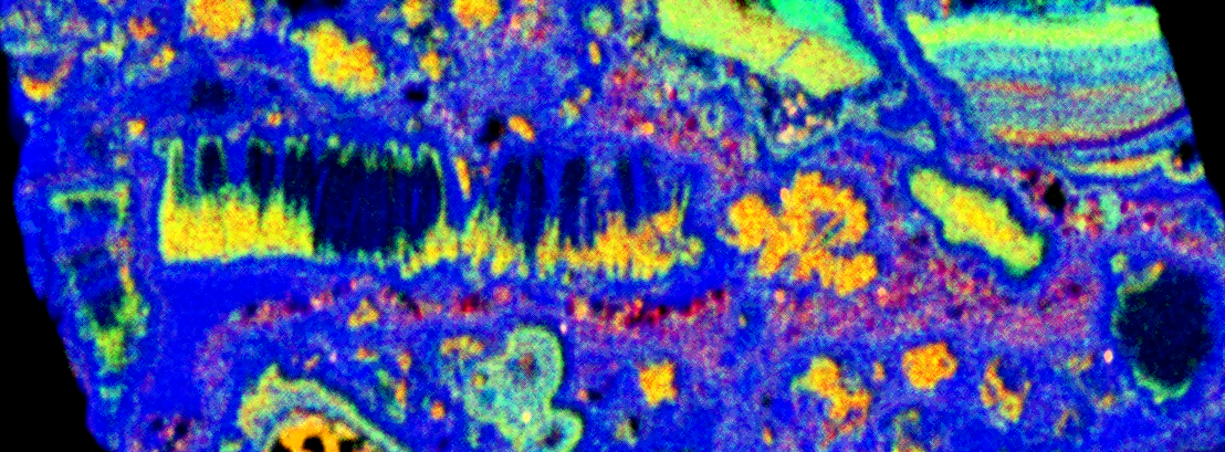
Analyze Topographic Samples at High-Resolution
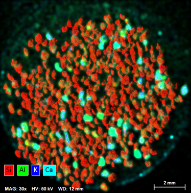
The visualization of topographic samples in the SEM becomes possible with Bruker’s Full Range EDS package, which contains an EDS detector and XTrace 2, which is equipped with a patent protected Aperture Management System (AMS). The AMS keeps the sample in focus even at variable working distances, allowing X-ray mapping at a micrometer resolution over a greater working distance. An example of a printed circuit board is shown.

Detect Elements Below a Sample's Surface
The high energy of the X-ray source used for Full Range EDS has the ability to reveal information from underneath the sample surface that is not detectable by conventional EDS. The information depth is element and matrix dependent and can range from micrometers up to even centimeters.
Full Range EDS can be used for elemental analysis both on and below a samples surface. In the example shown the gold wires and connections within a SD card can be resolved without having to remove its plastic coating.
Optical Image

Conventional EDS - Gold Map

Full Range EDS - Gold Map

As shown in this composite elemental map taken using Full Range EDS, excitation via micro-XRF allows for the complex internal structure of electronic devices to be easily investigated. This is especially useful in applications such as failure analysis and quality control.
Full Range EDS - Composite

Map Over Large Areas
Conventional large area EDS mapping using SEM stage movement can be hampered by imperfect image stitching, non-flat intensity profiles at the edge of each image and sample charging. In addition, only elements from the sample surface are visible. Bruker’s Full Range EDS package supplemented with Rapid Stage solves that problem. Rapid Stage moves the sample either underneath the fixed X-ray optic or e-beam, with no SEM stage movement required, so that large areas of the sample can be mapped in a single field measurement.
Rapid Stage allows users to map elemental data over large areas, dependent only on the size of the SEM sample chamber. The Rapid Stage itself can map an area of 45 x 45 mm without having to move the SEM stage.

Analyze Multi-Layered Samples
Full Range EDS provides film thickness analysis for multiple layer structures ranging from very thin nanometer thick layers up to several millimeter thick layers as photons are not limited to the sample surface and can pick up sample information from a greater depth.
Multi-layer analysis is particularly useful for the analysis of thin films, coatings, semiconductors, and electronics.

Want to learn more?
View more webinars on the QUANTAX Micro-XRF page.
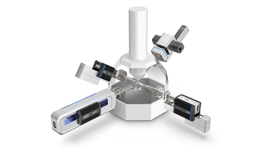
QUANTAX Micro-XRF - A System for Full Range EDS
QUANTAX Micro-XRF is Bruker's system that converts a conventional SEM EDS set-up into a dual-beam analytical system via the addition of an X-ray source.
Don't settle to work within the limits of conventional EDS. Unlock the full potential of EDS and discover more about your sample using QUANTAX Micro-XRF

Contact a Bruker Expert about our Analytical Solutions for Electron Microscopes
Thank you
Your request was successfully sent.