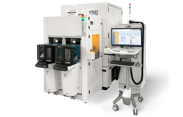
Automated AFM Metrology

InSight AFP

Fifth-generation AFP with industry’s highest resolution, fastest profiling, and rapid 3D die mapping

Inline Metrology

Preferred Choice of Leading Foundries and Memory Makers

Long-Term Stability and Productivity for Advanced Process Control and Development

InSight AFP is the world’s highest performance and industry preferred CMP profiling and etch depth metrology system for advanced technology nodes. The combination of its modern tip scanner with inherently stable capacitive gauges and an accurate air-bearing positioning system enables non-destructive, direct measurements in the active area of dies.

0.3 nm
long-term stability
Delivers NIST-traceable reference metrology with measured stability over one year
260 - 340 sites/hour
highest productivity for inline applications
Reduced MAM times and optimized wafer handling maintain up to 50 wafers/hour throughput
Up to 36,000 µm/sec
profiling speed
Provides high-resolution 3D characterization with hot-spot identification
Features

Highest Resolution with Longest Tip Life

InSight AFP's TrueSense® technology, with the proven long-scan capability of an atomic force profiler. Etch depth, dishing, and erosion on submicron features can be monitored fully automated with unsurpassed repeatability without relying on test keys or models. It’s unique 

Process

Fully-Automated, Inline Process Control for Etch and CMP Wafers

The Insight AFP combines the latest innovations in atomic force microscopy, including Bruker’s proprietary CDMode characterizing sidewall features and roughness.  CDmode reduces the amount of required cross-sectioning, realizing significant cost savings. In addtion, AFP data provides a direct side-wall roughness measurement that cannot be obtained through other techniques.  

Yield Improvement

Automated Defect Review and Classification

The device killing defects of today's leading ICs are smaller than ever and require rapid resolution for HVM demands. The InSight AFP provides fast, actionable topographical and material information about defects on semiconductor wafers and phtomasks that allows manufacturers to rapidly identify sources of defectivity and eliminate their impact on production.

100x high-resolution registration optics and AFM Global Alignment enable less than ± 250 nm raw image placement accuracy for patterned wafer and mask ensuring that the defect of interest is the defect measured.

The system is fully compatible with KLARITY and most other YMS systems.

R&D

3D Die Mapping and HyperMap™

After Polish Hot Spot Inspection - Scan Rate: 26 mm/sec; Number of scan lines: 33,000

Profiling speeds up to 36,000 µm/sec enables rapid, full 3D post-CMP  characterization and inspection for full 33 mm x 26 mm flash fields and larger. Sub 2 nm out-of-plane motion for true large-scale topography and fully automated post polish hot spot detection.

In this example a full, standard, 26 mm x 33 mm reticle field scan was acquired in 24 hours at 1 micron x 1 micron pixel size. Hot spots may then be automatically detected and rescanned using Bruker's Hot Spot Detection and Review capability.

Applications

What is your challenge?

Sub nm Profiling Sensitivity

CMP Advanced Process Control

Process control requires accuracy, precision and long-term reproducibility; CMP process control requires all of these while maintaining sensitivity to the sub nanometer topography of modern polishing technologies for front, mid, back and far-back end-of-line. The InSight AFP's picometer sensitivity ensures detection of post polish residual topography. With 2 picometer, long term, probe-to-probe repeatability and reproducibility, this is data to trust for process control.
High Aspect Ratio Depth Metrology

Etch Advanced Process Control

Etch depth metrology for process control, a simple, critical, ask; DTMode is the answer. DTMode is a Bruker proprietary adaptive scan mode, proven to have the lowest Total Measurement Uncertainty (TMU) of any AFM for depth metrology. With a < 10 s MAM time, DTMode enables the depth metrology required for HVM Etch process control.
NAND and Power Devices

Etch Process Development

Measure twice…. cut once. Metrology as part of process development is more critical than ever. Short loops, process variants and complex DOEs require metrology systems to be highly flexible and adaptable while maintaining the critical accuracy and precision requirements. The InSight AFP’s simple, intuitive recipe interface enables metrology for process development through an XML/CAD interface that enables recipe writing in < 5 min.
Logic and Memory

CMP Process Development

Metrology for CMP process development requires speed, accuracy, precision and all while permitting the flexibility required for robust recipes. The extended range, super-flat scanner has less than 1nm out of plan motion over the entire 105 μm scan range ensuring the highest accuracy metrology of the lowest topographies. Combining the extended range, 105 μm scanner with the Large Area Scanning mode enables metrology for CMP process development from 10s of nm to 300 mm.
New Metrics and New Challenges

Lithography EUV APC

The transition to EUV lithography has brought with it a number of new metrology metrics that must be monitored. One of these new metrics is Top Line Roughness (LTR). LTR does correlate with defectivity and yield results for the two resists discussed here. The resist with lower LTR (by 9% on average) develops significantly less line break defects and shows much better yield (Resist B). Therefore, LTR analyses post development may be used for early screenings of new resist formulations and help to forecast pitch- and dose-dependent performance as well as allow for yield predictions. The InSight AFP’s TrueSense™ mode provides the highest resolution AFM image for non-destructive Top Line Roughness EUV process monitoring
Non-Destructive Hybrid Metrology

Lithography EUV Process Development

E-beam resist shrinkage continues to be an issue for EUV resists. Characterizing and understanding how the resist profile changes with ebeam exposure is critical for developing the best models for EUV process development. The InSight AFP’s TrueSense™ mode is the solution to this challenge. TrueSense™ relies on instantaneous feedback enabling pico Newton force control ensuring the highest accuracy, non-destructive surface profiling. Measuring those areas that are exposed and areas that are not exposed characterizes the resist profile change. This additional data is then fed into the metrology kit to generate better models for faster process development. This requires that the AFP and the SEM are measuring the same exact features. This is enabled by sharing recipes through the XML interface and sub 250nm raw image placement accuracy.

Support

How Can We Help?

Bruker partners with our customers to solve real-world application issues. We develop next-generation technologies and help customers select the right system and accessories. This partnership continues through training and extended service, long after the tools are sold.

Our highly trained team of support engineers, application scientists and subject-matter experts are wholly dedicated to maximizing your productivity with system service and upgrades, as well as application support and training.

Contact Us

Input value is invalid.

* Please fill out the mandatory fields.

Please enter your first name
Please enter your last name
Please enter your e-mail address
Please enter a valid phone number
Please enter your Company/Institution
What best describes your current interest?
Please add me to your email subscription list so I can receive webinar invitations, product announcements and events near me.
Please accept the Terms and Conditions