
Nanostructural Characterization of Semiconductors with SEM
Quantitative Analysis of Nanostructured Semiconducting Materials in the Scanning Electron Microscope
This webinar will discuss the quantitative characterization of nanostructured semiconducting materials using Scanning Electron Microscope (SEM) with Energy Dispersive X-ray Spectroscopy (EDS) and Transmission Kikuchi Diffraction (TKD) techniques.
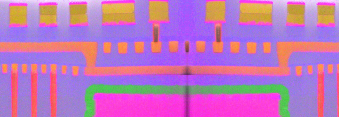
We will investigate the microstructure and elemental composition of multilayered semiconductor materials using FEG-SEM. Crystallographic information of these thin multilayers are useful to predict or enhance the physical, chemical, interfacial and electronic properties of such devices. However, their crystallographic study is challenging because these materials have complex and heterogenous architecture with ultrafine grain size and are e-beam sensitive. Here we present the benefit of using transmitted orientation contrast imaging and mapping with the SEM. Using application examples on CPU, SSD and CIGS solar cells, we demonstrate the analytical capabilities of on-axis TKD technique to characterize semiconducting multilayers at the nanoscale.
This webinar will conclude with a 15-minute Q&A session where our experts will answer your questions.


Speakers

Dr. Laurie Palasse
Global Application Manager, Bruker Electron Microscope Analyzers

Dr. Purvesh Soni
Sr. Applications Scientist EDS, Bruker Electron Microscope Analyzers



Watch this Webinar On-Demand
Please enter your details below to gain on-demand access to this webinar.