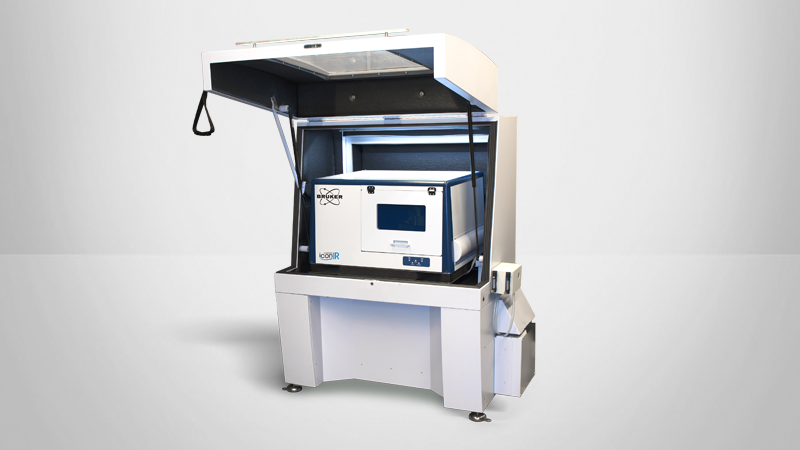
Large-Sample Dimension IconIR: Defect detection and Chemical-ID Characterization of Semiconductor Devices
Our experts demonstrate the capabilities of the IconIR for semiconductor materials research
PRESENTATION HIGHLIGHTS:
- [00:00:00] Welcome
- [00:02:27] An Introduction to the Dimension IconIR
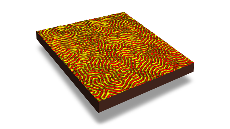
- [00:11:37] Applications in the Semiconductor Industry
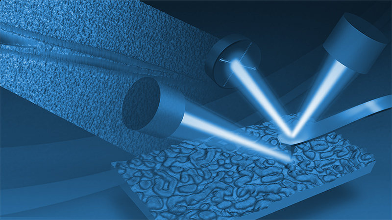
- [00:31:55] Demonstration of the Dimension IconIR
- [00:45:18] Q/A & Summary