On-Demand Session: Cutting Edge Imaging: Harnessing Diamond Probes for Advanced AFM Performance
Diamond Probes: Unique Material Advantages
PRESENTATION HIGHLIGHTS:
[00:00:40] Why Diamond as Tip Material?
[00:01:23] Diamond Tip Technologies
[00:02:25] Single Crystal diamond tips mounted on cantilevers
[00:03:05] CVD diamond coatings on Si tips
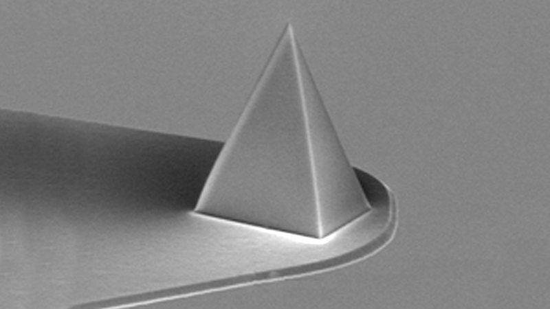
[00:04:35] Sharpened Single-Crystal Diamond Tips
[00:05:30] Sharpened / Shaped Single-Crystal Diamond Tips
High-Resolution Imaging with Excellent Probe Lifetime
PRESENTATION HIGHLIGHTS:
[00:00:11] Atomic Resolution in Vaccum
[00:01:58] Atomic Resolution in Air
[00:04:30] Low-roughness samples
[00:07:37] Cantilever Based Nano Indentation
[00:09:27] Nano Indentation on Polycarbonate Sample
[00:10:40] Nano Indentation Practical Aspects
[00:11:50] Nano Indentation Examples
[00:13:00] PeakForce QNM
[00:15:30] Contact Resonance Mapping
Electrical Imaging and Analysis with Conductive Diamond Probes
PRESENTATION HIGHLIGHTS:
[00:00:47] Scanning Spreading Resistance Microscopy
[00:04:50] Conductive AFM
[00:07:20] PeakForce TUNA
[00:08:06] Scanning Capacitance Microscopy (SCM)
[00:10:55] KPFM
[00:11:30] Piezoresponse Force Microscopy (PFM)
[00:12:27] Material Removal (Scalpel)
[00:14:45] Scalpel AFM
[00:16:00] Scalpel C-AFM (or Tomographic C-AFM)
[00:17:24] Scalpel SSRM
Question & Answer
PRESENTATION HIGHLIGHTS:
[00:00:00] If probe tips are being damaged or contaminated while scanning a rubber carbon black silica composite, would diamond probes help mitigate this issue?
[00:02:00] What is the best method for cleaning contaminated tips?
[00:04:05] Are these tips usable for living materials? What is the minimum force you can apply?