CH₃NH₃PbI₃ Perovskites: Ferroelasticity Revealed
Evgheni Strelcov, Qingfeng Dong, Tao Li, Jungseok Chae, Yuchuan Shao, Yehao Deng, Alexei Gruverman, Jinsong Huang, and Andrea Centrone
Key points
- AFM-IR was used to find evidence of ferroelasticity in CH3NH3PbI3 polycrystalline films and crystals
- No evidence of conomitant ferroelectricity was observed
- The configuration of ferroelastic domains can be controlled with applied stress
Abstract
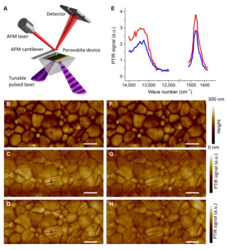
Ferroelectricity has been proposed as a plausible mechanism to explain the high photovoltaic conversion efficiency in organic-inorganic perovskites; however, convincing experimental evidence in support of this hypothesis is still missing. Identifying and distinguishing ferroelectricity from other properties, such as piezoelectricity, ferroelasticity, etc., is typically nontrivial because these phenomena can coexist in many materials. In this work, a combination of microscopic and nanoscale techniques provides solid evidence for the existence of ferroelastic domains in both CH3NH3PbI3 polycrystalline films and single crystals in the pristine state and under applied stress. Experiments show that the configuration of CH3NH3PbI3 ferroelastic domains in single crystals and polycrystalline films can be controlled with applied stress, suggesting that strain engineering may be used to tune the properties of this material. No evidence of concomitant ferroelectricity was observed. Because grain boundaries have an impact on the long-term stability of organic-inorganic perovskite devices, and because the ferroelastic domain boundaries may differ from regular grain boundaries, the discovery of ferroelasticity provides a new variable to consider in the quest for improving their stability and enabling their widespread adoption.
2D Materials and Nanophotonics

Nanoscale Infrared Spectroscopy
Measure spatially varying physical and chemical properties with nanoscale spatial resolution