NanoWizard V NanoScience
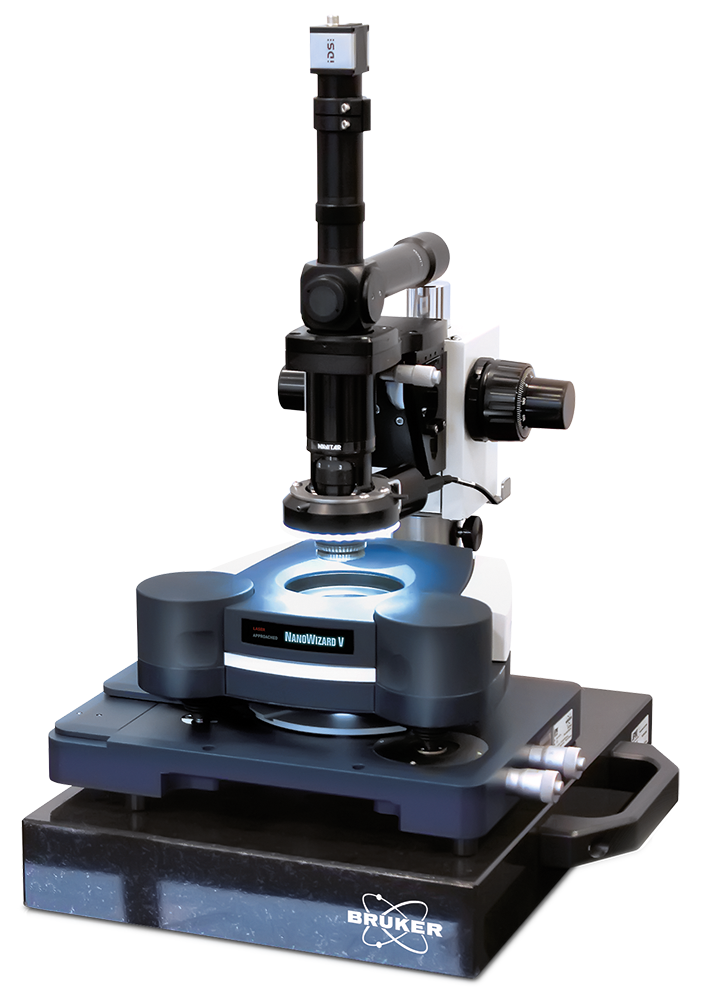
NanoWizard® V NanoScience
The NanoWizard® V combines high spatio-temporal resolution with a large scan area, flexible experiment design, and outstanding integration with advanced optical microscope systems. Its automated setup, alignment, and re-adjustment of system parameters opens new possibilities for long-term, self-regulating experiments series.
Discover the 5th Generation NanoWizard NanoScience AFM

Nanowizard® V sets a new benchmark in automation while providing a host of new technical capabilities and a degree of comfort second to none.
- Latest generation packed with novel innovations
- Proven legacy of success through an install base of nearly 1000 JPK/Bruker NanoWizard AFMs across the globe
- Supported by dedicated cantilever development for high-resolution imaging, fast scanning, and customized applications
- Intuitive V8 software environment
- Unmatched ease-of-use
- Ideal for multi-user imaging facilities
Perfected Performance and Increased Productivity
The NanoWizard V is an outstanding tool for the nanosciences, uniquely combining technical innovation with performance and user comfort.
Paving the way for new scientific discoveries
- Lowest noise scanner and detection system ensure high-resolution data and unrivalled performance
- High-speed scanning rates of up to 400 lines/sec
- Ideal for real-time investigation of dynamics
- Automation for improved productivity and maximized throughput
- High-resolution nanomechanical imaging with PeakForce-QI™, PeakForce Tapping®, PeakForce QNM,
and QI - DirectOverlay for AFM in conjunction with advanced optical microscopy
- Features the latest ExperimentPlanner and ExperimentControl options
- Widest range of accessories for environment control, electrical measurements and more
Superior Performance
- Versatile imaging from atomic lattices to large scale samples
- Largest range of add-ons
- Extended optical viewing field for AFM with tiling feature
- Optimized storage of parameters and favorite settings
- Intuitive user operation
- Standardized batch analysis routines for the generation of statistically relevant datasets
- Fully automated cantilever and detector alignment
- Capture fast dynamic processes in harsh environments
- Follow reactions across multiple time scales, from milliseconds, to seconds and minutes


Comprehensive Nanomechanical Characterization
Bruker continuously strives to improve the nanomechanical characterization capabilities of its AFMs and to provide easy technology solutions for complex scientific endeavors.
The NanoWizard V is the ideal solution for quantifying nanomechanical properties and understanding the crucial role they play in structure, morphology, and molecular interactions.
The NanoWizard V pushes the boundaries of science, opening the AFM technology to a wider range of applications and making nanomechanical characterization faster, easier, and more accessible for users of all fields of science.
Unrivalled Capabilities
- Fast scanning and ease-of-use combined with topographic and nanomechanical imaging
- Characterization of viscoelastic properties using microrheological measurements
- Contact resonance for mechanical characterization of stiff samples (>10 GPa)
- Intuitive and powerful RampDesigner software
- Highly sensitive force control and tip-saving features
- True, real-time force curve monitoring
- Mechanical mapping combined with electrical sample characterization in a single run
New Chapter in Quantitative Imaging
PeakForce-QI, the symbiosis of PeakForce Tapping and QI mode, delivers unique quantitative nanomechanical imaging capabilities. It combines highest acquisition rates with advanced force control to deliver highest resolution, multi-parametric images. The automated setup, operation, and calibration make it simple to configure and run an experiment, and obtain top-quality images and data quickly and easily, even for non-experts.
Powerful Data Analysis
- Easy, reliable batch processing
- Flexible creation of topography images at different forces
- Zero force (contact point) imaging Image stack output of any channel from batch processing


Automation and Intuitive Operation at Its Best
The NanoWizard V was designed to meet the specific needs of scientists in research and industry today. Innovative hardware and software solutions have led to increased throughput, automated measurement pro-cedures, and batch processing routines that allow scientists to focus on what’s important – their research.
Highest Level of Automation
- Automated alignment of laser detection system
- Automated cantilever calibration
- Automated multi-region imaging using HybridStage or motorized stage
- Intuitive scripting of automated experiments with ExperimentPlanner
- ExperimentControl for remote monitoring of experiments
Intuitive Operation
- Workflow-based software with fundamental ease-of-use features
- User management, ideal for multi-user facilities
- Integrated software assistance
- Single-click optical image calibration
- Integrated camera for alignment of laser detection system
- Comprehensive data processing routines
- Convenient saving of parameters and favorite settings


Unrivalled Flexibility by Design
The renowned tip-scanner technology and modular design of the NanoWizard V NanoScience AFM can be seamlessly integrated with advanced optical techniques.
A wide range of advanced modes and accessories make it the most flexible AFM available on the market today, enabling versatile experimental setups and environmental control.
Comprehensive Range of Add-ons and Accessories
- Broad range of temperature control accessories (-120 °C up to +300 °C)
- Scanning Thermal Microscopy (SThM)
- Magnetic Force Microscopy (MFM)
- Nanomanipulation
- Friction Force Microscopy
- Multimodal imaging
- Stretching stages
- Various fluid cells
- see accessories brochure for more options
High-Resolution Electrical Characterization
- Conductive AFM (CAFM)
- Kelvin Probe Force Microscopy (KPFM)
- Electrostatic Force Microscopy (EFM)
- Piezo Force Microscopy (PFM)
- Scanning Tunneling Microscopy (STM)
- Scanning Electrochemical Microscopy (SECM)
For Complex Experiments, from Polymers to Solar Cells
- Optimized environmental control options
- Optical accessibility of the sample, e.g., for defined illumination
- 980 nm detection laser option
- Various modes for long-term, unattended experiments


The New Benchmark for Fast Scanning of Large Samples
The NanoWizard V NanoScience platform delivers fast scanning over a large scan area. The full scan range in all three axes remains available, providing unparalleled scanning speeds and easy switching between sample features, without relocation of the sample or a reduction of imaging speed.
The Fast Scanning option is ideal for the investigation of dynamic processes, delivering the speed and accuracy necessary to study phenomena, such as crystallization, growth, melting, and domain building, in real time.
Innovative Fast Scanning Capabilities in an Automated AFM
- Improved productivity and maximized throughput for reliable statistics
- Fast z-piezo with high resonance frequency delivers fastest feedback
- Adaptive intelligence-based scanning routines enable scanning rates of up to 400 lines/sec
- NestedScanner technology provides fast scanning of corrugated samples with a z-range of up to 16.5 µm
- Active balancing allows fast scanning over large scan areas
High-Resolution Electrical Characterization
- Conductive AFM (CAFM)
- Kelvin Probe Force Microscopy (KPFM)
- Electrostatic Force Microscopy (EFM)
- Piezo Force Microscopy (PFM)
- Scanning Tunneling Microscopy (STM)
- Scanning Electrochemical Microscopy (SECM)
Stability and Highest Data Accuracy Meets Ease-of-Use
- Fast scanning with advanced closed-loop control
- Fast z-piezo equipped with capacitive sensor for highest data accuracy
- Accurate force control thanks to latest feedback technologies
- DirectDrive feature for increased cantilever excitation stability
- Batch processing and advanced data analysis routines
- Movie creator

NanoWizard NanoScience Data Gallery
Bruker’s BioAFMs allow life science and biophysics researchers to further their investigations in the fields of cell mechanics and adhesion, mechanobiology, cell-cell and cell-surface interactions, cell dynamics, and cell morphology. We have collected a gallery of images demonstrating a few of these applications.
Operating Modes
Standard Operating Modes
- Now with PeakForce-QI including PeakForce Tapping, QI and PeakForce QNM
- Including fast PeakForce Tapping and QI with nested scanner technology
- Contact mode with lateral force microscopy (LFM)
- Tapping Mode™ with PhaseImaging™
- ExperimentPlanner for designing a specific measurement workflow
- Static and dynamic force spectroscopy
- Advanced Force Mapping
Optional Modes
- Advanced spectroscopy modes such as various force clamp modes or ramp designs
- Fast scanning option with line rates of up to 200 Hz
- QI Advanced mode for quantitative data, perfect for soft samples
- ScanAsyst automated gain and setpoint adjustment in PeakForce Tapping and PeakForce-QI
- Advanced AC modes such as FM and PM with Q-control & Active Gain Control
- Microrheology in CellMech Package
- Kelvin Probe Microscopy
- MFM and EFM
- Conductive AFM
- STM
- Electrical spectroscopy modes
- Piezoresponse Microscopy for high voltages
- Electrochemistry & Scanning Electrochemistry with temperature control and optical microscopy
- NanoLithography and NanoManipulation
- NanoIndentation
- Scanning Thermal AFM
- FluidFM® solution from Cytosurge
- ExperimentControl feature for remote experiment control
- DirectOverlay 2 for combined AFM and optical microscopy
- Additional XY or Z sample movement stages available with CellHesion®, TAO and HybridStage module
The Widest Range of Accessories in the Market
Optical systems/accessories, electrochemistry solutions, electrical sample characterization, environmental control options, software modules, temperature control, acoustic and vibration isolation solutions and more. Bruker provides you with the right accessories to control your sample conditions and to perform successful experiments.
Accessories to extend your BioAFM capabilities
Bruker offers an extensive range of BioAFM system add-ons, accessories, and modes to deliver maximum experimental and sample control, superior versatility, and enhanced useability. These options extend the range of applications and experiments supported by Bruker BioAFMs far beyond what is possible with any other BioAFM system on the market today.
Available options include optical systems/accessories, electrochemistry solutions, electrical sample characterization, environmental control options, software modules, temperature control, acoustic and vibration isolation solutions, and more.
Browse our online accessories database or download our accessories handbook to learn more.

Watch Recent BioAFM Webinars
Our webinars cover best practices, introduce new products, provide quick solutions to tricky questions, and offer ideas for new applications, modes, or techniques.
Testimonials
"The performance of NanoWizard AFMs is exceptional. In the NanoWizard V, Bruker have built on this with automated alignment and fast imaging even at large scan sizes, solving real user problems. This instrument will expand the range of experiments possible and make what were once difficult experiments routine."
Dr Nic Mullin
Senior Experimental Officer for the Biophysical Imaging Centre Department of Physics and Astronomy, Sheffield, UK
