NanoWizard V NanoScience
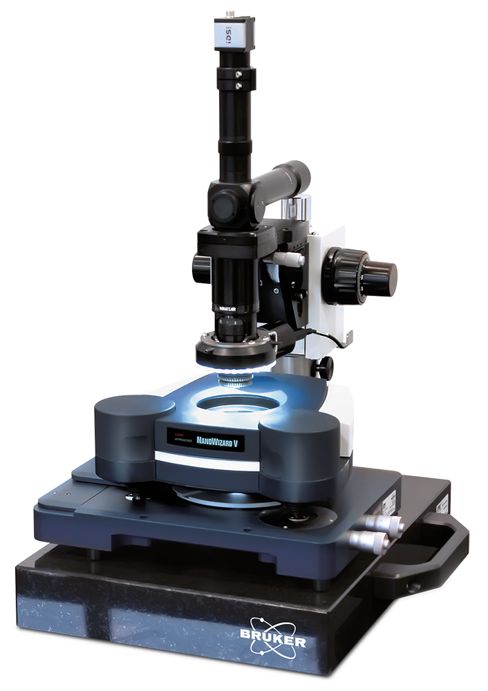
NanoWizard® V NanoScience
NanoWizard® V 는 높은 시공간 분해능과 큰 스캔 영역, 유연한 실험 설계, 첨단 광학 현미경 시스템과의 탁월한 통합을 결합합니다. 시스템 매개 변수의 자동 설정, 정렬 및 재조정을 통해 장기적이고 자체 조절적인 일련의 실험이 가능하도록 새로운 가능성을 열어줍니다.
5세대 NanoWizard NanoScience AFM 알아보기

Nanowizard® V는 수많은 새로운 기술 기능과 최고의 편의성을 제공하는 동시에 자동화 분야에서 새로운 벤치마크를 설정합니다.
- 새로운 혁신으로 가득한 최신세대
- 전 세계적으로 약 1,000개의 JPK/Bruker NanoWizard AFM 설치 기반을 통해 검증된 성공 사례
- 고해상도 이미징, 고속 스캔 및 맞춤형 애플리케이션을 위한 전용 캔틸레버 개발이 지원
- 이해하기 쉬운V8 소프트웨어 환경
- 탁월한 사용 편의성
- 다중 사용자 이미징 시설에 이상적
완벽한 성능 및 생산성 향상
NanoWizard V 는 기술 혁신과 성능 및 사용자 편의성을 독특하게 결합한 나노과학을 위한 뛰어난 도구 입니다.
새로운 과학적 발견을 위한 개척
- 최저 소음 스캐너 및 감지 시스템으로 고해상도 데이터와 탁월한 성능 보장
- 초당 최대 400회선의 고속 스캔 속도
- 역학을 실시간으로 조사하는 데 이상적임
- 자동화를 통해 생산성 향상 및 처리량 극대화for improved productivity and maximized throughput
- PeakForce-QI™, PeakForce Tapping®, PeakForce QNM 및 QI를 사용한 고해상도 나노역학적 이미징
- 고급 광학 현미경과 함께 사용되는 AFM의 DirectOverlay
- 최신ExperimentPlanner 와ExperimentControl 옵션 포함
- 환경 제어, 전기 측정 등을 위한 광범위한 액세서리
탁월한 성능
- 원자 격자에서 대형 샘플에 이르기까지 다양한 이미징
- 광범위한 추가 기능
- 타일링 기능이 있는 AFM용 확장 광학 시야
- 매개 변수 및 즐겨찾기 설정의 최적화된 스토리지
- 이해하기 쉬운 사용자 작업
- 통계적으로 관련된 데이터 세트 생성을 위한 표준화된 배치 분석 루틴
- 완전 자동화된 캔틸레버 및 검출기 설정
- 가혹한 환경에서 신속한 동적 프로세스 포착
- 밀리초에서 몇 초, 몇 분까지 다양한 시간 척도에서 반응 추적


포괄적인 나노역학적 특성화
브루커는 AFM의 나노역학적 특성화 기능을 개선하고 복잡한 과학적 노력을 위한 쉬운 기술 솔루션을 제공하기 위해 지속적으로 노력하고 있습니다.
NanoWizard V 는 나노역학적 특성을 정량화하고 구조, 형태학 및 분자 상호작용에서 중요한 역할을 이해하는 데 이상적인 솔루션입니다.
NanoWizard V는 과학의 경계를 넓혀 AFM 기술을 더 넓은 범위의 응용 분야에 개방하고 나노기계적 특성화를 모든 과학 분야의 사용자를 위해 더 빠르고, 더 쉽고, 더 접근하기 용이하게 합니다.
타의 추종을 불허하는 기능
- 지형 및 나노 역학 이미징과 결합된 빠른 스캐닝 및 사용 편의성
- 미세유동학 측정을 이용한 점탄성 성질 특성화
- 강성 시료의 기계적 특성화를 위한 접촉공진(>10 GPa)
- 이해하기 쉽고 강력한 RampDesigner 소프트웨어
- 매우 민감한 힘 제어 및 팁 절약 기능
- 정확한 실시간 힘 곡선 모니터링
- 단일 실행에서 전기 샘플 특성화와 결합된 기계적 매핑
정량 이미지의 새로운 장
PeakForce Tapping과 QI 모드의 공생인 PeakForce-QI는 고유한 정량적 나노기계 이미징 기능을 제공한다. 높은 습득율과 고급 힘 제어를 결합하여 고 해상도, 다중 파라미터 이미지를 제공합니다. 자동화된 설정, 작동 및 조정은 구성을 간단하게 하고 실험을 실행하고, 전문가가 아닌 사람도 고품질 이미지와 데이터를 빠르고 십게 얻을 수 있도록 합니다.
강력한 데이터 분석
- 쉽고 안정적인 배치 처리
- 다양한 힘으로 지형 이미지를 유연하게 생성
- 제로포스(접점) 이미징. 배치처리에서 채널의 이미지 스택 출력


최고의 자동화 및 이해하기 쉬운 운영
NanoWizard V NanoWizard V는 오늘날 연구와 산업에 종사하는 과학자들의 특정한 요구를 충족시키기 위해 설계되었습니다. 획기적인 하드웨어 및 소프트웨어 솔루션은 과학자들이 중요한 연구에 집중할 수 있도록 처리량, 자동화된 측정 절차 및 배치 처리 루틴을 증가시켰습니다.
최고 수준의 자동화
- 레이저 감지 시스템의 자동 정렬
- 자동 캔틸레버 조정
- HybridStage또는 모터 구동 스테이지를 사용한 자동화된 다중 영역 이미징
- Experiment Planner를 사용한 자동 실험의 이해하기 쉬운 스크립터
- 실험 원격 모니터링을 위한 ExperimentControl
이해하기 쉬운 작동
- 기본적인 사용 편의성 기능을 갖춘 워크플로우 기반 소프트웨어
- 다중 사용자 기능에 적합한 사용자 관리
- 통합 소프트웨어 지원
- 클릭 한 번으로 광학 이미징 조정
- 레이저 감지 시스템의 정렬을 위한 통합 카메라
- 포괄적인 데이터 처리 루틴
- 매개 변수 및 즐겨찾기 설정의 편리한 저장


Unrivalled Flexibility by Design
The renowned tip-scanner technology and modular design of the NanoWizard V NanoScience AFM can be seamlessly integrated with advanced optical techniques.
A wide range of advanced modes and accessories make it the most flexible AFM available on the market today, enabling versatile experimental setups and environmental control.
Comprehensive Range of Add-ons and Accessories
- Broad range of temperature control accessories (-120 °C up to +300 °C)
- Scanning Thermal Microscopy (SThM)
- Magnetic Force Microscopy (MFM)
- Nanomanipulation
- Friction Force Microscopy
- Multimodal imaging
- Stretching stages
- Various fluid cells
- see accessories brochure for more options
High-Resolution Electrical Characterization
- Conductive AFM (CAFM)
- Kelvin Probe Force Microscopy (KPFM)
- Electrostatic Force Microscopy (EFM)
- Piezo Force Microscopy (PFM)
- Scanning Tunneling Microscopy (STM)
- Scanning Electrochemical Microscopy (SECM)
For Complex Experiments, from Polymers to Solar Cells
- Optimized environmental control options
- Optical accessibility of the sample, e.g., for defined illumination
- 980 nm detection laser option
- Various modes for long-term, unattended experiments


The New Benchmark for Fast Scanning of Large Samples
The NanoWizard V NanoScience platform delivers fast scanning over a large scan area. The full scan range in all three axes remains available, providing unparalleled scanning speeds and easy switching between sample features, without relocation of the sample or a reduction of imaging speed.
The Fast Scanning option is ideal for the investigation of dynamic processes, delivering the speed and accuracy necessary to study phenomena, such as crystallization, growth, melting, and domain building, in real time.
Innovative Fast Scanning Capabilities in an Automated AFM
- Improved productivity and maximized throughput for reliable statistics
- Fast z-piezo with high resonance frequency delivers fastest feedback
- Adaptive intelligence-based scanning routines enable scanning rates of up to 400 lines/sec
- NestedScanner technology provides fast scanning of corrugated samples with a z-range of up to 16.5 µm
- Active balancing allows fast scanning over large scan areas
High-Resolution Electrical Characterization
- Conductive AFM (CAFM)
- Kelvin Probe Force Microscopy (KPFM)
- Electrostatic Force Microscopy (EFM)
- Piezo Force Microscopy (PFM)
- Scanning Tunneling Microscopy (STM)
- Scanning Electrochemical Microscopy (SECM)
Stability and Highest Data Accuracy Meets Ease-of-Use
- Fast scanning with advanced closed-loop control
- Fast z-piezo equipped with capacitive sensor for highest data accuracy
- Accurate force control thanks to latest feedback technologies
- DirectDrive feature for increased cantilever excitation stability
- Batch processing and advanced data analysis routines
- Movie creator

NanoWizard NanoScience Data Gallery
Bruker’s BioAFMs allow life science and biophysics researchers to further their investigations in the fields of cell mechanics and adhesion, mechanobiology, cell-cell and cell-surface interactions, cell dynamics, and cell morphology. We have collected a gallery of images demonstrating a few of these applications.
Operating Modes
Standard Operating Modes
- Now with PeakForce-QI including PeakForce Tapping, QI and PeakForce QNM
- Including fast PeakForce Tapping and QI with nested scanner technology
- Contact mode with lateral force microscopy (LFM)
- Tapping Mode™ with PhaseImaging™
- ExperimentPlanner for designing a specific measurement workflow
- Static and dynamic force spectroscopy
- Advanced Force Mapping
Optional Modes
- Advanced spectroscopy modes such as various force clamp modes or ramp designs
- Fast scanning option with line rates of up to 200 Hz
- QI Advanced mode for quantitative data, perfect for soft samples
- ScanAsyst automated gain and setpoint adjustment in PeakForce Tapping and PeakForce-QI
- Advanced AC modes such as FM and PM with Q-control & Active Gain Control
- Microrheology in CellMech Package
- Kelvin Probe Microscopy
- MFM and EFM
- Conductive AFM
- STM
- Electrical spectroscopy modes
- Piezoresponse Microscopy for high voltages
- Electrochemistry & Scanning Electrochemistry with temperature control and optical microscopy
- NanoLithography and NanoManipulation
- NanoIndentation
- Scanning Thermal AFM
- FluidFM® solution from Cytosurge
- ExperimentControl feature for remote experiment control
- DirectOverlay 2 for combined AFM and optical microscopy
- Additional XY or Z sample movement stages available with CellHesion®, TAO and HybridStage module
The Widest Range of Accessories in the Market
Optical systems/accessories, electrochemistry solutions, electrical sample characterization, environmental control options, software modules, temperature control, acoustic and vibration isolation solutions and more. Bruker provides you with the right accessories to control your sample conditions and to perform successful experiments.
Accessories to extend your BioAFM capabilities
Bruker offers an extensive range of BioAFM system add-ons, accessories, and modes to deliver maximum experimental and sample control, superior versatility, and enhanced useability. These options extend the range of applications and experiments supported by Bruker BioAFMs far beyond what is possible with any other BioAFM system on the market today.
Available options include optical systems/accessories, electrochemistry solutions, electrical sample characterization, environmental control options, software modules, temperature control, acoustic and vibration isolation solutions, and more.
Browse our online accessories database or download our accessories handbook to learn more.

Watch Recent BioAFM Webinars
Our webinars cover best practices, introduce new products, provide quick solutions to tricky questions, and offer ideas for new applications, modes, or techniques.
Testimonials
"The performance of NanoWizard AFMs is exceptional. In the NanoWizard V, Bruker have built on this with automated alignment and fast imaging even at large scan sizes, solving real user problems. This instrument will expand the range of experiments possible and make what were once difficult experiments routine."
Dr Nic Mullin
Senior Experimental Officer for the Biophysical Imaging Centre Department of Physics and Astronomy, Sheffield, UK
