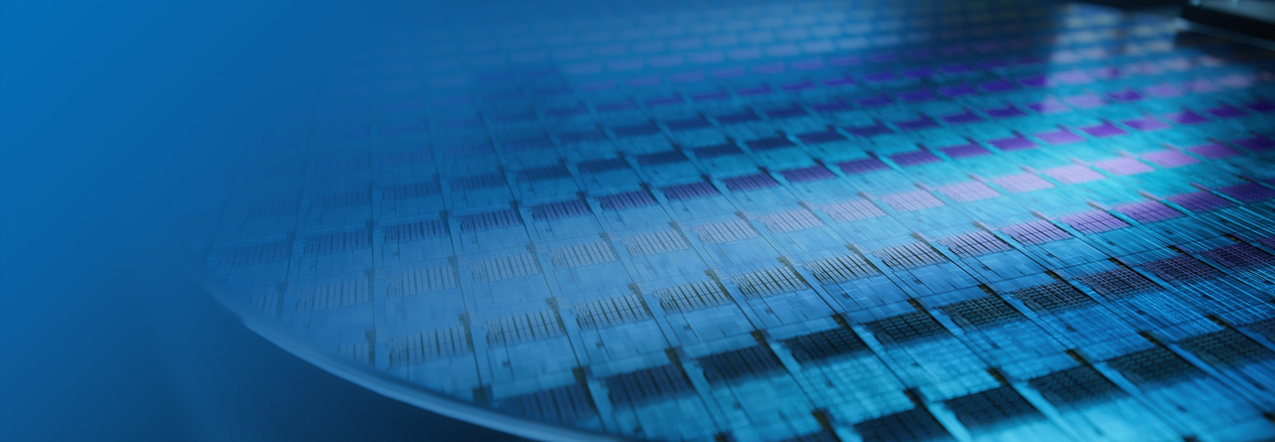
Surface Metrology Systems
Lab-to-Fab Surface Characterization
Bruker provides advanced metrology solutions for characterizing semiconductor materials, interfaces, structures, and advanced packaging features across research, process development, and manufacturing environments.
These solutions combine high-resolution mechanical, adhesion, dimensional, and topographical measurements with advanced optical inspection capabilities to address a wide range of semiconductor characterization challenges. From nanomechanical property and interfacial adhesion measurements to advanced packaging inspection, defect review, profile metrology, and structural characterization, Bruker's portfolio delivers the measurement sensitivity, precision, and automation required for today's most demanding semiconductor applications. Automated workflows, high-throughput operation, and compatibility with development and production environments help streamline process optimization and product improvement.
These technologies help semiconductor manufacturers gain deeper insight into material behavior, process performance, and device structures to accelerate development, improve yield, and support advanced manufacturing requirements.
Find the Best Surface Metrology Solution for You
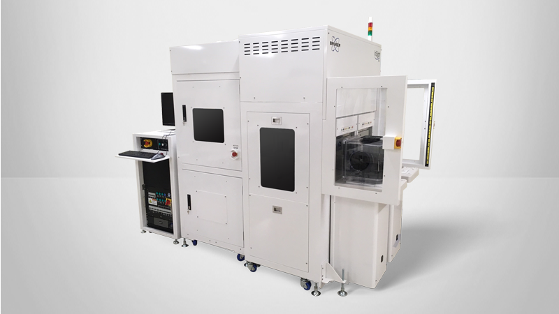
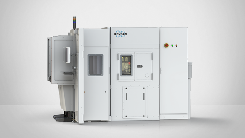
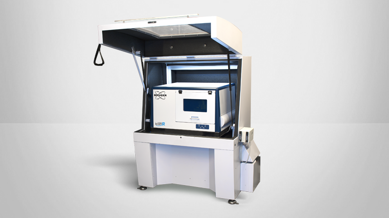
White Light Interferometry and Stylus Profilometry Systems
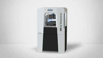
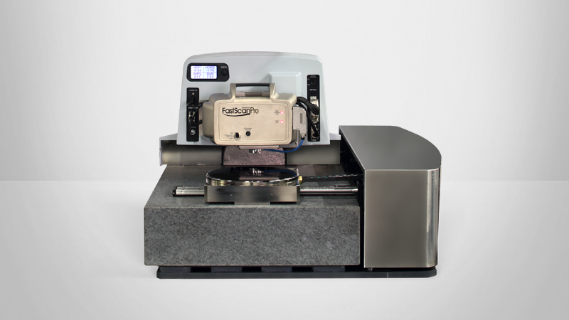
Nanomechanical Testing and Tribology
Nanoscale Property and Chemical Characterization
Advanced Metrology Solutions for Semiconductor Manufacturing Applications
From process development to quality assurance, understanding surfaces is an essential part of semiconductor device manufacturing. Bruker’s surface metrology solutions support advanced packaging, nanomechanical metrology, process monitoring, defect detection, and nanoscale characterization applications across semiconductor manufacturing environments.
To learn more, contact us to discuss your measurement requirements, find out about the systems best-suited for your application, discuss options for system specialization, or request a quote based on your specific needs.

Advanced Packaging, Bonding, & Interconnect Metrology
Support advanced packaging processes and critical package structures with high-accuracy metrology and characterization capabilities.
- Die flatness and CMP metrology for advanced packaging
- TSV and interconnect measurements
- QA/QC metrology for fan-out process
- Wafer bonding

Surface Topography, Thickness, & Stress Analysis
Qualify and quantify surface topography to analyze film thickness, stress, surface roughness, and form.
- Surface roughness characterization, step height measurements, and film stress analyses

Mechanical Property, Interfacial Adhesion, & CMP Characterization
Measure thin film mechanical properties, interfacial adhesion, and CMP-related performance for process development and consumables characterization.
- Automated thin film mechanical and interfacial adhesion metrology
- Complete characterization of CMP processes and consumables

Process Monitoring, Defect Detection, & Nanoscale Characterization
Support process control, defect review, critical dimension measurements, and nanocontaminant identification for advanced semiconductor materials and devices.
- Inline and near-line process monitoring
- Hot-spot and defect detection on full reticle die
- Critical dimension measurements
- Nanocontaminant identification
Frequently Asked Questions
Bruker’s surface characterization solutions support a broad range of semiconductor applications, including die flatness and CMP metrology for advanced packaging, TSV and interconnect measurements, automated thin film mechanical and interfacial adhesion metrology, inline and near-line process monitoring, hot-spot and defect detection on full reticle die, complete characterization of CMP processes and consumables, surface roughness characterization, step height measurements and film stress analyses, and QA/QC metrology for fan-out processes.
From process development to quality assurance, understanding surfaces is an essential part of semiconductor device manufacturing. Bruker offers metrology solutions for advanced packaging, process monitoring, defect detection, thin film mechanical property measurements, interfacial adhesion metrology, surface roughness characterization, film stress analysis, and nanoscale characterization applications.
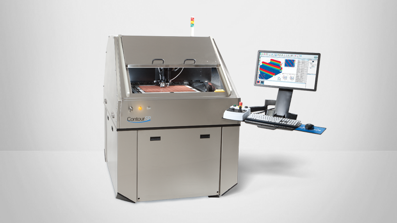
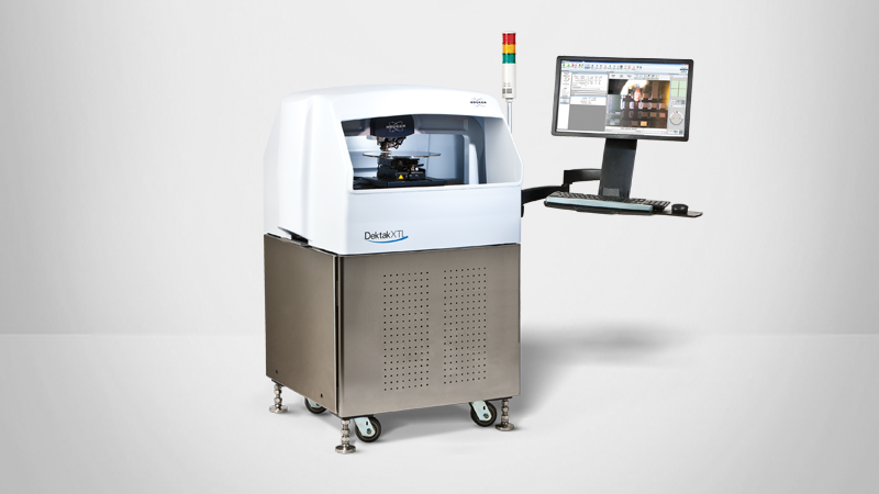
Profilometry is used to qualify and quantify the topography of surfaces, enabling analysis of film thickness, stress, surface roughness, form, and more. Bruker’s white light interferometry systems provide magnification-insensitive resolution, high throughput, and the ability to measure trench sidewalls, delivering applications ranging from CMP optimization and layer stacking to wafer bonding and advanced packaging.
Bruker’s Hysitron Nanomechanical Metrology Tools provide automated metrology solutions that deliver high-speed, high-resolution, highest-sensitivity mechanical property and interfacial adhesion measurements, streamlining nanomechanical property sampling and supporting persistent product and process improvement.
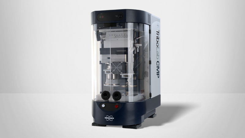
Bruker offers multiple technologies for CMP characterization and process development. Surface metrology solutions support die flatness and CMP metrology for advanced packaging and complete characterization of CMP processes and consumables, while TriboLab tribometers and mechanical testers provide a versatile means to investigate friction, wear, load, hardness, and lubrication for CMP consumables and process development.
Atomic force microscopy (AFM) is used to characterize nanoscale topographical, mechanical, electrical, magnetic, thermal, and coupled properties of advanced materials. Bruker’s AFM platforms can be customized for applications such as critical dimension measurements and carrier profile characterization, while AFM‑IR enables nanochemical insights and identification of the chemistry, properties, and process origin of nanocontaminants.
Bruker’s surface metrology technologies support process development, quality assurance, process monitoring, defect detection, advanced packaging metrology, thin film mechanical property characterization, interfacial adhesion measurements, and nanoscale characterization. Together, these capabilities help support product and process improvement across semiconductor manufacturing applications.
How Can We Help?

Service and Application Support to Optimize Tool Utilization
The decision to invest in high-performance metrology is based on more than instrument performance and price. Bruker is committed to keeping your tool running at the peak of up-time and productivity. We have a highly educated worldwide team of service and support personnel that takes great pride in first-time solution of issues. Our variety of service coverage programs can be customized to match your specific requirements, including optimization of tool performance, recipe writing, and in-person technical support visits.
Bruker tailors services to your needs:
- Priority technical support
- Advance replacement parts and assemblies stored in regional warehouses for rapid response times
- Application and training services
Get Expert Answers
Ask us a question, request more information, or get in touch with a Bruker sales representative.