Knowledge Pack: 3D Optical Profiler Characterization of Thin Films
Get instant access to technical resources on using 3D optical profilometry for thin‑film thickness and surface characterization, spanning fundamentals, application‑level use cases, and practical measurement guidance.
This knowledge pack includes:
- 3 full-length application notes with measurement examples and case data
- 2 video lessons covering principles, accuracy, and applications
- 2 real-time video demos showing thin‑film thickness and surface texture measurements
+ on-demand access to all presentations from our Thin Films & Coatings Symposium
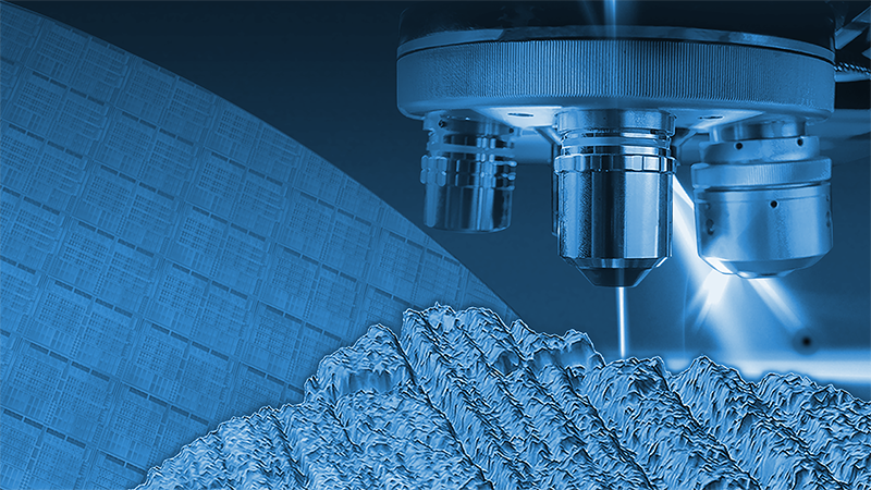
Thin Film Characterization with 3D Optical Profilometry
3D optical profilometry enables non‑contact, high‑resolution measurement of thin‑film thickness and surface topography across a wide range of materials and structures. This collection of resources includes technical fundamentals and comparisons, application notes, and real‑time demonstrations that show how 3D optical profiling is applied in practical thin‑film workflows, when it is the appropriate metrology choice, and how to interpret optical surface data with confidence in research, process development, and manufacturing environments.
Our most popular resources, from measurement fundamentals to practical demos
This collection provides technical resources on 3D optical profilometry based on white‑light interferometry (WLI) for thin‑film thickness and surface characterization, spanning:
- WLI measurement fundamentals for thin‑film applications
- Film thickness and surface texture measurement with 3D optical profiling
- Comparison of WLI with other thin‑film metrology techniques
- Real‑world measurement workflows for opaque and transparent films and challenging geometries
- Application‑level case studies and live demos of real‑time film thickness measurement

Video: Introduction, Technology Refresher, and Basic Film Measurement Workflows
RESOURCE TYPE: Video (part 1 of our Thin Films & Coatings Symposium; full on-demand symposium access with knowledge pack)
LENGTH: ~10 minutes
DESCRIPTION:
Bruker applications specialists introduce the core principles of 3D optical profilometry for thin‑film and coated‑surface characterization. The discussion focuses on what the technique measures, how measurements are performed, and how results are interpreted in thin‑film applications. Emphasis is placed on establishing consistent terminology, conceptual grounding, and a clear understanding of how optical surface data supports thin‑film analysis.
VIEWERS WILL LEARN:
- How white‑light interferometry works for thin‑film measurement
- What surface parameters a 3D optical profiler measures
- How thin‑film measurements are acquired and interpreted
- Core terminology and concepts used across optical surface metrology

Application Note: Thickness Measurements of Opaque and Transparent Films or Coatings with WLI
RESOURCE TYPE: Application Note [PDF]
LENGTH: 4 pages
DESCRIPTION:
This application note details the measurement physics and configurations used to determine thin‑film thickness with WLI. It describes how interference signals from the film surface and substrate are used to calculate thickness, and how measurement strategies differ for opaque versus transparent films. Illustrative example data is included to reinforce the fundamentals and show how thickness values are derived and validated.
READERS WILL LEARN:
- How to derive film thickness from WLI interference signals
- Differences between opaque and transparent film measurement strategies
- When step‑height vs through‑film measurements are appropriate
- How to interpret example thickness measurement data

Video: Full‑Area Optical Surface Texture Measurement with 3D Optical Profilers
RESOURCE TYPE: Video (part of our UK Surface Metrology Workshop; full on-demand workshop access with knowledge pack)
LENGTH: ~30 minutes
DESCRIPTION:
Bruker metrology specialists place 3D optical profilometry (WLI) within the broader context of surface metrology. The discussion compares WLI with stylus scanning, confocal microscopy, and focus variation, highlighting differences in contact vs non‑contact measurement, data density, and applicable surface types. Accuracy, vertical and lateral measurement scales, and achievable resolution are explained, with real use cases — such as ranking surface finishing processes and calculating wear volume — used to demonstrate practical applicability.
VIEWERS WILL LEARN:
- How WLI compares to stylus, confocal, and focus‑variation techniques
- Vertical and lateral scales captured by 3D optical profiling
- Accuracy and resolution considerations for surface texture measurement
- Practical examples including finishing‑process ranking and wear‑volume calculation

Application Note: Performing Comprehensive Wafer Inspection with Non‑Contact 3D Optical Profiling
RESOURCE TYPE: Application Note [PDF]
LENGTH: 4 pages
DESCRIPTION:
This application note explores how 3D optical profilometry scales to wafer‑level inspection, integrating thin‑film measurement into broader semiconductor device and packaging workflows. Using real inspection data, the note shows how full‑field optical measurements capture multiple surface parameters simultaneously and support efficient, non‑contact inspection of thin films on patterned and fragile wafers.
READERS WILL LEARN:
- How WLI is applied to wafer‑scale inspection
- How thin‑film measurements fit into device and packaging workflows
- What surface parameters can be extracted from a single scan
- Practical considerations for non-contact wafer inspection

Application Note: Characterization of CMP Processes with White Light Interferometry
RESOURCE TYPE: Application Note [PDF]
LENGTH: 6 pages
DESCRIPTION:
This application note presents a process‑focused case study showing how WLI is used to characterize thin‑film surfaces before and after chemical mechanical planarization (CMP). Before‑and‑after measurement data is used to quantify changes in surface topography and connect surface topography changes to process performance and outcomes.
READERS WILL LEARN:
- How WLI is applied to CMP process evaluation
- How surface topography changes are quantified before and after CMP
- How measurement data is used to compare process conditions
- How optical profiling relates to CMP performance outcomes

Demo: Measuring Thickness of a Sellotape/Kapton Tape Film
RESOURCE TYPE: Real-time technical demonstration
LENGTH: ~10 minutes
DESCRIPTION:
In this expert‑led demonstration, Bruker specialists apply WLI measurement concepts to a real thin‑film sample, using a Sellotape/Kapton tape multi-layer film to show how measurements are executed and interpreted in practice. The demo reinforces how optical profiler data is collected, visualized, and analyzed, serving as a concrete “see it in action” example following the conceptual and application‑level content.
VIEWERS WILL LEARN:
- How WLI measurements are performed on a real film sample
- How to interpret surface and film‑related data
- How theoretical concepts translate into practical measurement steps
- Common considerations when analyzing thin‑film measurement results

Demo: Transparent Thin‑Film Thickness Measurement
RESOURCE TYPE: Real-time technical demonstration
LENGTH: ~35 minutes
DESCRIPTION:
Bruker applications experts demonstrate real‑time thin‑film thickness measurement using WLI on a transparent coating applied to the inside of a soda can. Bruker metrology experts walk through instrument and software setup, live data acquisition, fringe identification, and thickness calculation, demonstrating how interference signals from the film surface and substrate are separated and combined to determine film thickness on a curved, internal surface.
VIEWERS WILL LEARN:
- How to configure hardware and software for transparent‑film thickness measurement
- How interference fringes from film and substrate are identified and separated
- How thickness is calculated from optical signal differences
- How WLI handles transparent films and challenging geometries