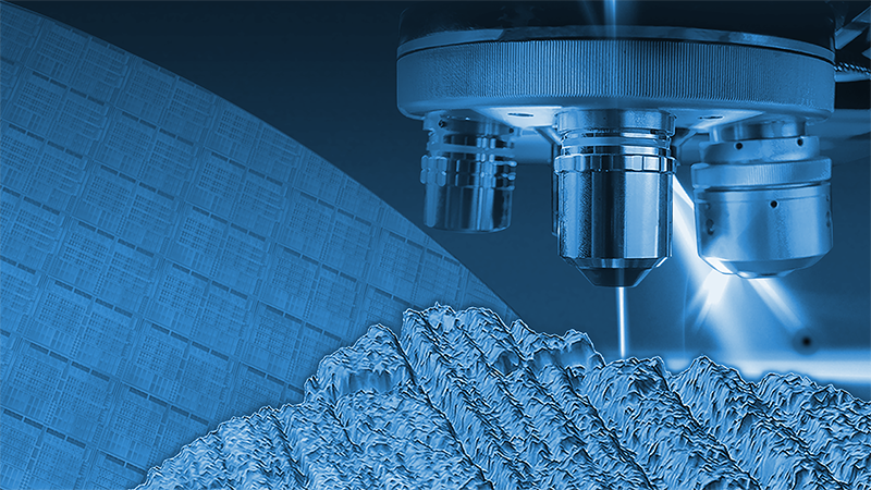
Knowledge Pack: 3D Optical Profiler Characterization of Thin Films

Thickness Measurements of Opaque and Transparent Films or Coatings with WLI
RESOURCE TYPE: Application Note [PDF]
LENGTH: 4 pages
DESCRIPTION:
This application note details the measurement physics and configurations used to determine thin‑film thickness with WLI. It describes how interference signals from the film surface and substrate are used to calculate thickness, and how measurement strategies differ for opaque versus transparent films. Illustrative example data is included to reinforce the fundamentals and show how thickness values are derived and validated.
READERS WILL LEARN:
- How to derive film thickness from WLI interference signals
- Differences between opaque and transparent film measurement strategies
- When step‑height vs through‑film measurements are appropriate
- How to interpret example thickness measurement data
Full‑Area Optical Surface Texture Measurement with 3D Optical Profilers
RESOURCE TYPE: Video
LENGTH: ~30 minutes

Performing Comprehensive Wafer Inspection with Non‑Contact 3D Optical Profiling
RESOURCE TYPE: Application Note [PDF]
LENGTH: 4 pages
DESCRIPTION:
This application note explores how 3D optical profilometry scales to wafer‑level inspection, integrating thin‑film measurement into broader semiconductor device and packaging workflows. Using real inspection data, the note shows how full‑field optical measurements capture multiple surface parameters simultaneously and support efficient, non‑contact inspection of thin films on patterned and fragile wafers.
READERS WILL LEARN:
- How WLI is applied to wafer‑scale inspection
- How thin‑film measurements fit into device and packaging workflows
- What surface parameters can be extracted from a single scan
- Practical considerations for non-contact wafer inspection

Characterization of CMP Processes with White Light Interferometry
RESOURCE TYPE: Application Note [PDF]
LENGTH: 6 pages
DESCRIPTION:
This application note presents a process‑focused case study showing how WLI is used to characterize thin‑film surfaces before and after chemical mechanical planarization (CMP). Before‑and‑after measurement data is used to quantify changes in surface topography and connect surface topography changes to process performance and outcomes.
READERS WILL LEARN:
- How WLI is applied to CMP process evaluation
- How surface topography changes are quantified before and after CMP
- How measurement data is used to compare process conditions
- How optical profiling relates to CMP performance outcomes
Measuring Thickness of a Sellotape/Kapton Tape Film
RESOURCE TYPE: Real-time technical demonstration
LENGTH: ~10 minutes
Transparent Thin‑Film Thickness Measurement
RESOURCE TYPE: Real-time technical demonstration
LENGTH: ~35 minutes