Ellipsometry and Reflectometry Systems
Advanced Optical Metrology Solutions from R&D to Production
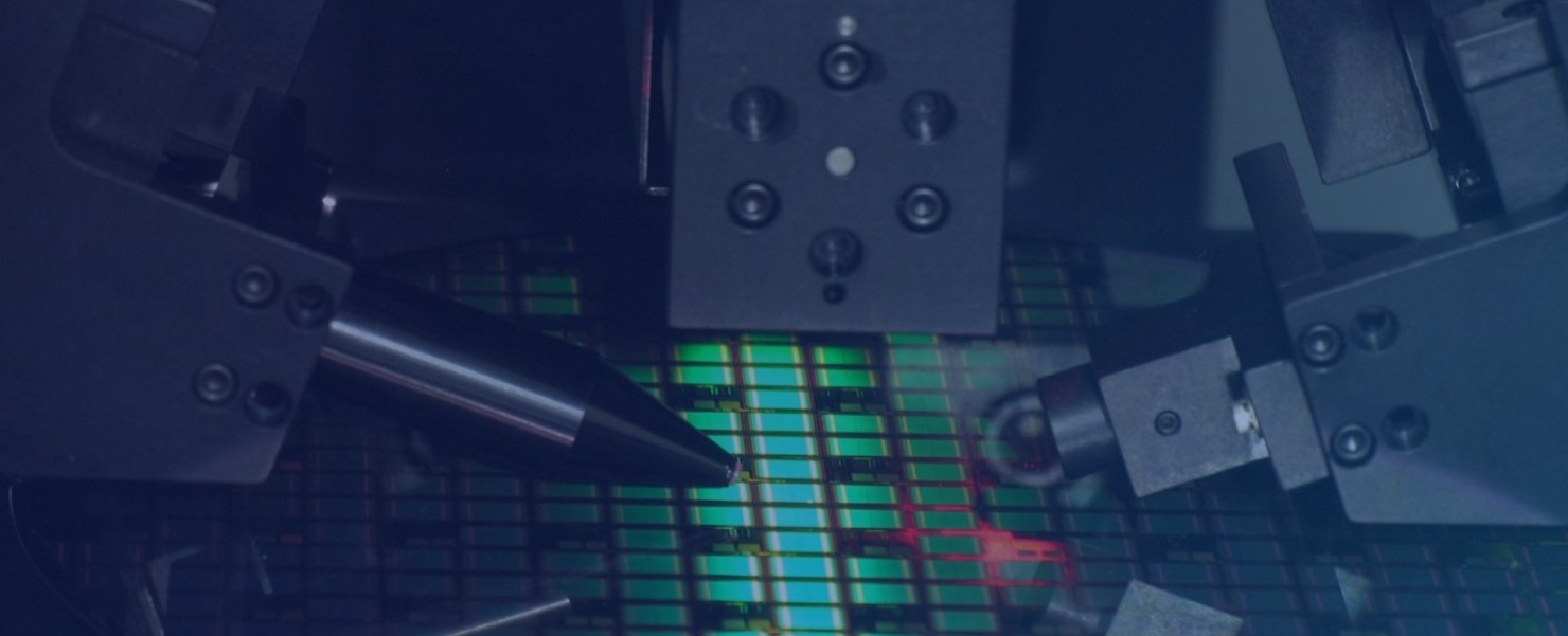
Based on non-contact optical techniques, FilmTek tools simultaneously measure multiple-angle and multi-modal data to determine film thickness and refractive index. By measuring multiple angles of incidence, a wavelength shift is introduced between spectra collected at different angles. The wavelength shift between the spectra is only a function of the refractive index of the film and the angle difference between the spectra. By independently determining refractive index from a wavelength shift (as opposed to extracting index information from amplitude changes), FilmTek tools have best-in-class performance for film thickness and refractive index measurement. This level of performance allows FilmTek tools to address applications that otherwise may not be possible with more conventional ellipsometry or reflectometry methods.
Contact us or request a quote to discuss your unique measurement needs with a Bruker applications expert.
Find the Best Film Metrology Solution for You
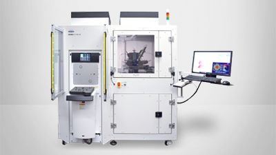
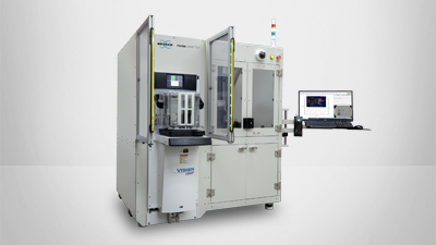
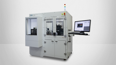
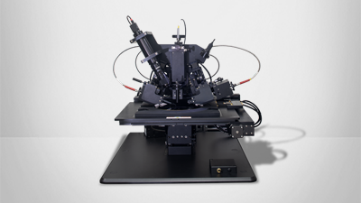
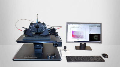
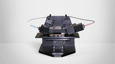
Stand-Alone Models
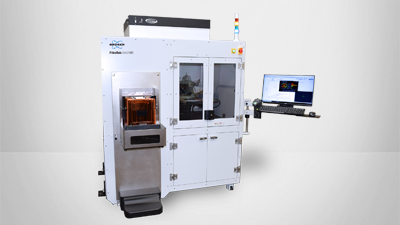
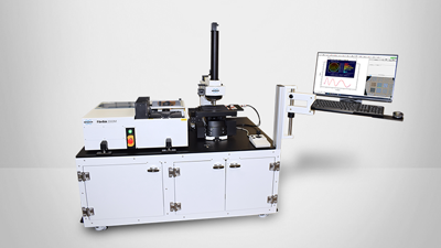
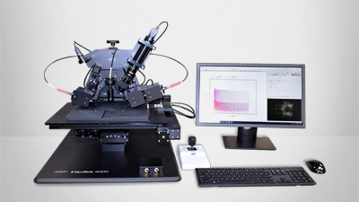
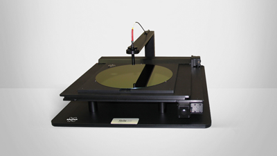
Benchtop Models
Contact us to discuss your measurement requirements, find out about the systems best-suited for your application, discuss options for system specialization, or request a quote based on your specific needs..
With installed systems in the world’s top development labs and industrial production floors, these metrology tools boast the highest accuracy and refractive index resolution for many thick, thin, and multilayer film applications that are not feasible with other metrology systems and are suited for use in settings ranging from academic research and R&D to high-volume manufacturing in controlled environments.
To support the broadest range of applications, samples, and environments, FilmTek systems are available in a variety of standard and customizable configurations. These range from manual benchtop instruments to fully automated production-line-ready models and include both single-technique and multimodal systems that combine our core technologies and additional technical integrations.
Advanced Thin Film Metrology with Application-Specific Solutions

Front End Semiconductors
Perform fast, accurate, and repeatable multi-layer film thickness and refractive index measurements on patterned device wafers for front end semiconductor manufacturing.
FilmTek systems enable process control of oxides, nitrides, ONO, Oxide / Nitride / Cu, polysilicon / oxide, AlN, TaN, TiN, SiGex and composition control, resist, Si3N4/GaAs, ARC, gate oxide, and GaAs films, CMP on Cu, and many other materials encountered throughout the entire wafer fabrication process.
RECOMMENDED SYSTEMS:

Advanced Packaging
Measure the complete range of back-end manufacturing and process control packaging parameters.
FilmTek process control solutions enable fully automated measurements for thick resist thickness for bump coplanarity, high-aspect-ratio TSV depth and top CD for interconnects, bonded silicon thickness or Total Thickness Variation (TTV), and thin metal-oxide thickness in bonding processes to prevent non-wet open failures.
RECOMMENDED SYSTEMS:

Silicon Photonics
Measure film thickness and refractive index with a 10x performance advantage over the best prism coupler contact systems.
Filmtek non-contact multi-angle reflectometry systems deliver precise high-resolution measurements and enable automated, in-line process control for a wide range of planar waveguide and silicon photonics applications (e.g., SiON, Si3N4, Ge-SiO2, P-SiO2, BPSG, APOX, HiPOX, and multi-layer SiO2/ SiON film stacks).
RECOMMENDED SYSTEMS:

Multi-layer Thin Films
Collect accurate, precise production measurements of thin films and multi-layers on patterned device wafers for front and back-end manufacturing.
Filmtek advanced multi-angle and multi-modal technology enables in-line composition control (e.g., %Ge in SiGex) for thin films, Oxide / Nitride / Cu, CMP process monitoring, and measurement of thin metal oxide thickness (SnO, CuO, InO) with sub-Angstrom repeatability to prevent non-wet open failures in bonding processes.
RECOMMENDED SYSTEMS:

Medical Sensors & Devices
Enhance the quality, consistency, and performance of medical devices and sensors with accurate and robust thickness measurement of biologically active films.
FilmTek thin film metrology instruments enable automated non-contact measurement and whole-wafer mapping of film thickness for glucose sensors, coating thickness mapping on the surface of metal jaws, and film thickness determination for multi-layer stacks in single-use blood sensors.
RECOMMENDED SYSTEMS:

MEMS
Perform fully-automated film thickness and refractive index measurements of oxide, nitride, oxide/nitride, ONO, amorphous carbon, resist, and oxide/polysilicon/oxide films on patterned device wafers.
Fully-automated FilmTek ellipsometry and reflectometry tools feature cassette-to-cassette wafer handling, 50µm spot size, pattern recognition, and SECS/GEM with a best-in-class combination of performance and price.
RECOMMENDED SYSTEMS:

Transparent Substrates
Accurately and uniquely determine thickness and optical constants of thin absorbing films on transparent substrates.
FilmTek reflection and transmission spectrophotometry systems enable non-contact optical characterization of virtually all translucent films ranging in thickness from less than 100 Å to approximately 150 µm with very high accuracy and repeatability. Typical measurement applications include ITO, NPB, Alq3, Si3N4, SiO2, polysilicon, a-Si, and multi-layer structures.
RECOMMENDED SYSTEMS:

New Materials
Characterize new materials with a wide range of rapid, accurate, and reliable R&D measurement capabilities.
FilmTek benchtop tools with automated wafer mapping enable measurements of multiple layer thicknesses, indices of refraction [n(λ)], extinction (absorption) coefficients [k(λ)], energy band gap [Eg], composition (e.g., %Ge in SiGex, % Ga in GaxIn1-xAs, %Al in AlxGa1-xAs, etc.), surface roughness, constituent / void fraction, crystallinity / amorphization (e.g., degree of crystallinity of Poly-Si or GeSbTe films), and film gradient.
RECOMMENDED SYSTEMS:

Unknown/Complex Materials
Independently and unambiguously determine thickness (t), refractive index (n), and extinction coefficient (k) for unknown materials.
FilmTek combined multiple-angle reflectometry and rotating compensator design ellipsometry systems deliver unprecedented performance with high-throughput automated mapping of patterned and un-patterned samples, 0.03 Angström repeatability for thin films, an extended thickness range from bare substrate to 50µm, and sub-Angström accuracy for complex, multi-layer thin film structures.
RECOMMENDED SYSTEMS:
Learn More About Our Technology


How Can We Help?

Bruker partners with our customers to solve real-world application issues. We develop next-generation technologies and help customers select the right system and accessories. This partnership continues through training and extended service, long after the tools are sold.
Our highly trained team of support engineers, application scientists and subject-matter experts are wholly dedicated to maximizing your productivity with system service and upgrades, as well as application support and training.
Get Expert Support
Ask us a question, request more information, or get in touch with a Bruker sales representative.