Nanomanipulation
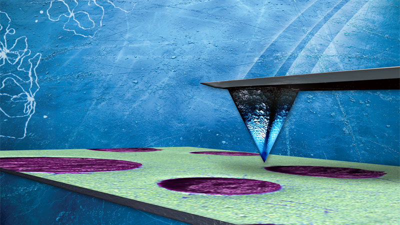
Through a set of nanomanipulation operating modes, AFM can also be applied for precise manipulation, modification, or fabrication of nanometer‑scale structures. Most nanomanipulation methods make use of precise force control to alternate between imaging the sample and modifying it. A nanomanipulation experiment typically consists of a series of alternating imaging and modification steps using the same tip.
During nanomanipulation operation, the tip follows a user‑defined path created by a series of user‑selected positions, vector files, or scripts. While following the path, the operating mode (contact mode or TappingMode) and related tip‑sample force interactions are precisely controlled to manipulate local sample features. Additional control of voltages can also be applied. Manipulation is typically followed by an imaging step (using the same probe) of the modified area.
Nanomanipulation is typically applied to move nanoparticles, nanowires, and other nanoscale objects that are loosely bound to the surface. A semiconductor industrial application for nanomanipulation is defect removal on EUV photomasks.
